Essential Terms for Sputtering and Evaporation Processe

Terminologies of Sputtering Coating

General Term

  1. Vacuum deposition: A group of methods used to deposit layers of material under a vacuum.
  2. Substrate: The material on which the film is deposited.
  3. Coating material: The raw material used to deposit the film, including sputtering targets and evaporation pellets materials.
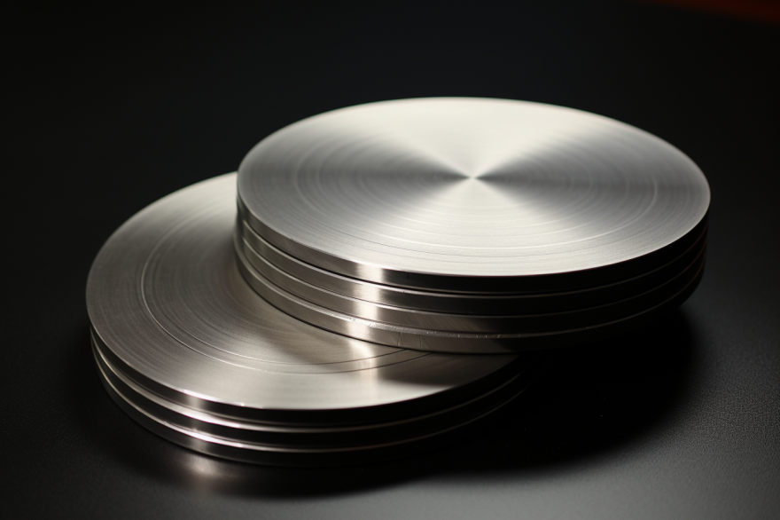
  4. Sputtering target: A coating material used for sputtering in vacuum sputtering.
  5. Sputtering rate: The amount of sputtering material used over a given time interval divided by the time interval.
  6. Deposition rate: The amount of material deposited on the substrate over a given time interval divided by the time interval and the surface area of ​​the substrate.

Information from SAM Sputter Target, a global coating materials supplier.

Technical Terminology

  1. Vacuum sputtering: The process by which inert gas ions bombard atoms (molecules) or radicals from the target surface in a vacuum.
  2. Reactive vacuum sputtering: Vacuum sputtering of film material of a desired chemical composition by reaction with a gas.
  3. Direct current diode sputtering: A direct current voltage between two electrodes causes the gas to self-sustain and discharge the target as a cathode.
  4. High-frequency diode sputtering: A high-frequency discharge is obtained by a high-frequency voltage between two electrodes to cause sputtering of a negative potential at a target.
  5. Ion beam sputtering: An ion beam obtained by a special ion source causes the sputtering of a target.
  6. Magnetron sputtering: The secondary electrons are bound to specific areas of the target surface using an orthogonal electromagnetic field formed on the surface of the target to enhance ionization efficiency and increase ion density and energy. Therefore, a very high sputtering rate can be obtained at a low voltage and a large current.

Special Parts

  1. Sputtering device: The components of a vacuum sputtering apparatus including a target and an auxiliary device necessary for sputtering (for example, a power supply device, a gas introduction device, etc.).
  2. Sputtering Target: The surface is bombarded with particles. The meaning of the target in this standard is the electrode composed of the sputtering material in the sputtering apparatus.
  3. Shutter: A device used to limit the coating in time and/or space and thereby achieve a certain film thickness distribution. The baffle can be either fixed or movable.
  4. Mask: A device used to cover part of the substrate and to limit the coating in space.
  5. Substrate heating device: A device that can heat a substrate or substrates to the desired temperature by heating in a vacuum coating device.
  6. Substrate cooling device: In a vacuum coating device, a device achieves the desired temperature by cooling a substrate or substrates.

Terminologies of Vacuum Evaporation

General Term

  1. Vacuum coating: A method of making a film on a substrate under vacuum.
  2. Substrate: The surface on which the film is deposited.
  3. Testing substrate: A substrate used for measurement and/or testing at the beginning of coating, during the coating process, and after coating.
  4. Coating material: The raw material used to make the film, mainly including sputtering targets and evaporation pellets materials.
  5. Evaporation material: A coating material used for evaporation in vacuum evaporation.
  6. Film material: the material constituting the film layer.
  7. Evaporation rate: the amount of material evaporated during a given time interval divided by
  8. Deposition rate: The amount of material deposited on a substrate over a given time interval divided by the time interval and the surface area of ​​the substrate.
  9. Coating angle: The angle between the direction of the particles incident on the substrate and the normal to the surface being plated.

Information from SAM Sputter Target, a global coating materials supplier.

Technical Terminology

  1. Vacuum evaporation coating: A vacuum coating process for evaporating a coating material.
  2. Simultaneous evaporation: Vacuum evaporation of various evaporation materials simultaneously onto the substrate by several evaporators.
  3. Evaporation field evaporation: Evaporation of a material evaporated from the evaporation field onto a substrate for evaporation (this process is applied to large-area evaporation to obtain a desired film thickness distribution).
  4. Reactive vacuum evaporation: Vacuum evaporation of film material of a desired chemical composition by reaction with a gas.
  5. Reactive vacuum evaporation in evaporator: Reacts with various evaporation materials in the evaporator to obtain vacuum evaporation of the desired chemical composition film material.
  6. Direct heating evaporation: The heat necessary to evaporate the evaporation of the material is the same as the heat of the evaporation material (in the crucible or not).
  7. Induction heating evaporation: The evaporation material is heated by induction eddy current.
  8. Electron beam evaporation: evaporation of heated material by electron bombardment.
  9. Laser beam evaporation: evaporation of the material by laser beam heating.
  10. Indirect heating evaporation: In a heating device (for example, a boat-shaped evaporator, a crucible, a filament, a heating plate, a heating rod, a spiral coil, etc.), the evaporation material is subjected to the heat necessary for evaporation, and is transferred to the evaporation material by heat conduction or heat radiation.
  11. Flash evaporation: intermittently evaporate a very small amount of evaporating material.

Special Parts

  1. Coating chamber: A part of a vacuum coating equipment that performs the actual coating process.
  2. Evaporator device: A vacuum coating device that includes an evaporator and all components necessary for its operation (such as power supply, supply, cooling devices, etc.).
  3. Evaporator: A device that evaporates directly within it, such as a boat-shaped evaporator, crucible, filament, heating plate, heating rod, spiral coil, etc., and if necessary, the evaporation material itself.
  4. Evaporator by direct heat: An evaporator in which the evaporation material itself is heated.
  5. Evaporator by indirect heat: An evaporator in which an evaporation material is heated by heat conduction or heat radiation.
  6. Evaporation field: A field formed by heating the same vaporized material by several arrays of evaporators.

Enhancing PV Device Efficiency with Indium Sputtering Targets

Introduction

Indium sputtering targets play a crucial role in the fabrication of photovoltaic (PV) devices, enhancing solar energy conversion efficiency. In this article, we discuss the advantages and applications of indium sputtering targets in improving the performance of PV devices.

Transparent Conductive Oxide (TCO) Layers

Indium sputtering targets are used to deposit high-quality indium tin oxide (ITO) films onto solar cells. These transparent conductive oxide layers offer excellent electrical conductivity and allow for light transmission, enhancing solar energy conversion efficiency.

Anti-Reflective Coatings

Indium sputtering targets enable the deposition of indium oxide or indium-tin-oxide thin films as anti-reflective coatings. These coatings minimize reflection losses, optimizing light absorption in PV devices and increasing overall energy conversion efficiency.

Back Contact Layers

Indium sputtering targets are utilized in depositing back contact layers in PV devices. These layers, made of indium or indium-containing compounds, improve charge collection and extraction, leading to enhanced power output and device performance.

Doping Layers

With indium sputtering targets, indium-containing films can be deposited as doping layers in PV devices. Doping with indium allows for better control of carrier concentration, facilitating efficient charge separation and collection, and improving solar energy conversion efficiency.

Conclusion

The use of indium sputtering targets in PV device fabrication enhances solar energy conversion efficiency. By enabling the deposition of transparent conductive oxide layers, anti-reflective coatings, back contact layers, and doping layers, indium sputtering targets optimize various aspects of PV device performance. As solar energy gains prominence as a clean and renewable energy source, the demand for indium sputtering targets in PV applications will continue to grow, driving further advancements in solar energy conversion technology.

For more information about indium sputter targets or other types of sputtering materials, please visit https://www.sputtertargets.net/.

Properties, Fabrication, and Applications of Indium Sputtering Targets in Thin Film Deposition

Introduction

Indium is a soft silvery-white metal that possesses unique properties, making it a valuable material in various fields of science and industry. One of the primary applications of indium is in thin film deposition. In this article, we will explore the properties of indium sputtering targets, their fabrication methods, and their wide-ranging applications in thin film deposition processes.

Properties of Indium Sputtering Targets

Indium sputtering targets exhibit several key properties that make them suitable for thin film deposition:

  1. Purity: High-purity indium sputtering targets are essential to ensure the quality and reliability of the deposited films. Typically, indium targets with purity levels greater than 99.99% are used to minimize impurities and enhance film performance.
  2. Density and Homogeneity: The density and homogeneity of the sputtering target play a vital role in achieving uniform film deposition. Indium targets with high density and excellent homogeneity ensure consistent film thickness and composition across the substrate.
  3. Grain Structure: The grain structure of indium sputtering targets affects their thermal and electrical conductivity. Fine-grained indium targets promote better electrical contact and heat transfer during the sputtering process, leading to improved film properties.

Fabrication of Indium Sputtering Targets

The fabrication process of indium sputtering targets involves the following steps:

  1. Melting and Casting: High-purity indium is melted in a controlled environment to remove any impurities. The molten metal is then cast into solid ingots or other desired shapes, such as discs or rectangles, depending on the specific requirements of the thin film deposition system.
  2. Hot/Cold Rolling: The cast indium ingots undergo hot or cold rolling processes to achieve the desired thickness and dimensions for sputtering target manufacturing. This step helps in improving the density and homogeneity of the indium targets.
  3. Annealing: Annealing is performed to relieve any residual stress and enhance the mechanical properties and grain structure of the indium sputtering targets. Controlled heating and cooling processes are employed to ensure optimal annealing conditions.
  4. Machining: The rolled and annealed indium sheets are machined to obtain the final shape and size of the sputtering target. Precision machining techniques such as cutting, grinding, and polishing are employed to achieve the required surface finish and dimensional accuracy.

Applications of Indium Sputtering Targets in Thin Film Deposition

Indium sputtering targets find wide-ranging applications in various thin film deposition techniques, including:

  1. Optoelectronic Devices: Indium tin oxide (ITO) films deposited using indium sputtering targets are extensively used in touchscreens, flat panel displays, and solar cells due to their excellent electrical conductivity and optical transparency.
  2. Semiconductor Industry: Indium sputtering targets are employed in the deposition of indium-based compounds, such as indium gallium arsenide (InGaAs), indium phosphide (InP), and indium antimonide (InSb), which are crucial for advanced semiconductor devices like high-speed transistors and infrared detectors.
  3. Superconducting Films: Indium sputtering targets are utilized in the deposition of superconducting films, specifically indium-based superconductors, which exhibit zero electrical resistance at low temperatures. Such films are significant in the development of high-performance electronic devices and quantum computing applications.
  4. Transparent Conductive Films: Indium sputtering targets are also employed to deposit transparent conductive films on glass or plastic substrates. These films find applications in organic light-emitting diodes (OLEDs), smart windows, and electromagnetic shielding films.

Conclusion

Indium sputtering targets offer valuable properties for thin film deposition, including high purity, density, homogeneity, and fine grain structure. The fabrication process ensures the production of high-quality targets suitable for diverse applications in optoelectronics, semiconductors, superconductors, and transparent conductive films. As technology advances, the demand for indium sputtering targets is likely to grow, contributing to further innovations in thin film deposition and related industries.

For more information about indium sputter targets or other types of sputtering materials, please visit https://www.sputtertargets.net/.