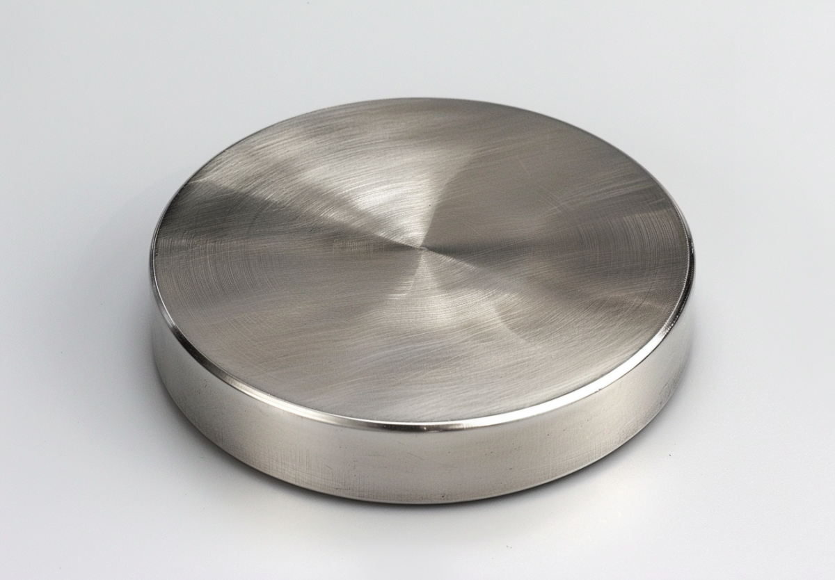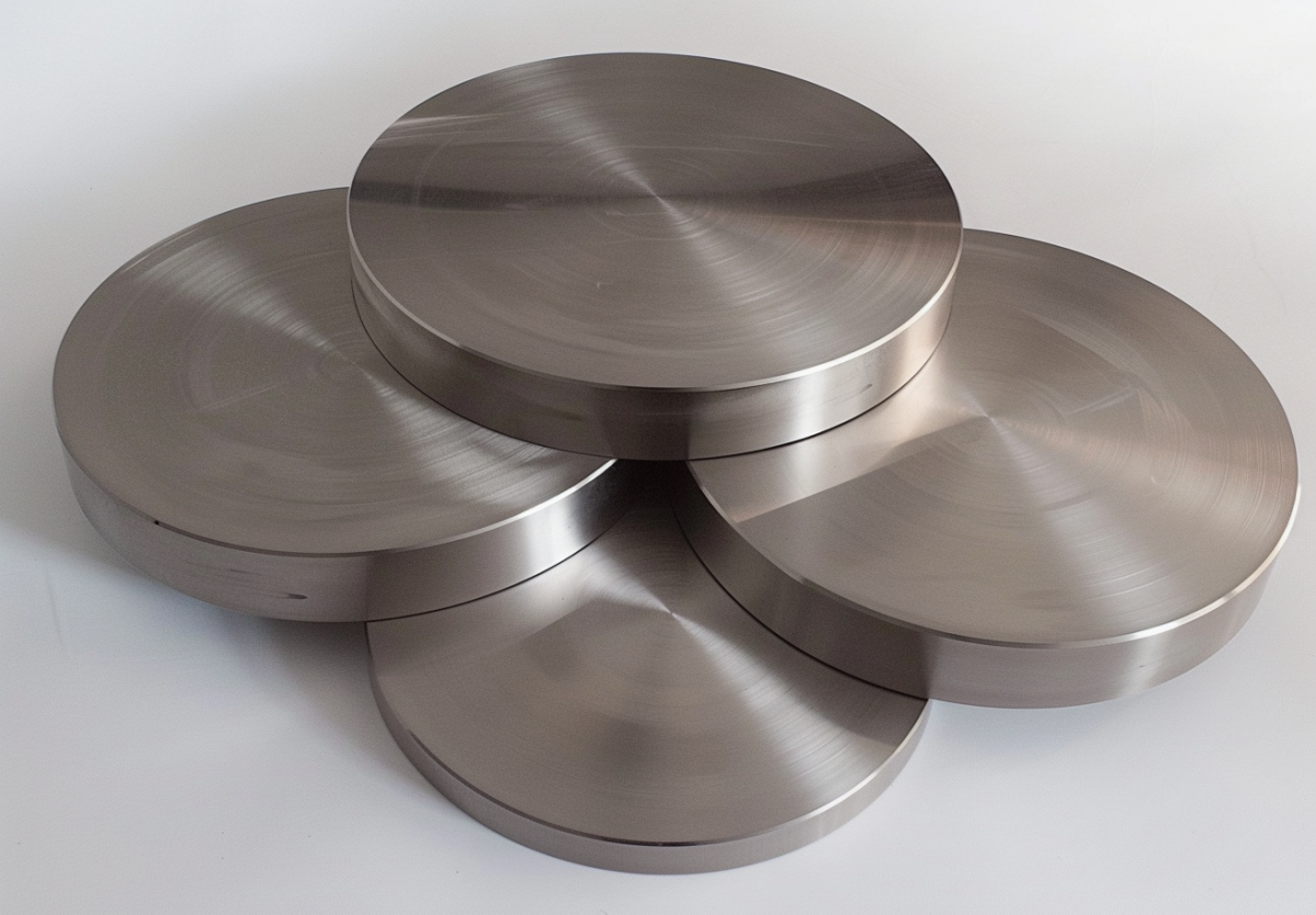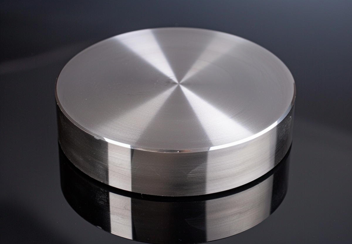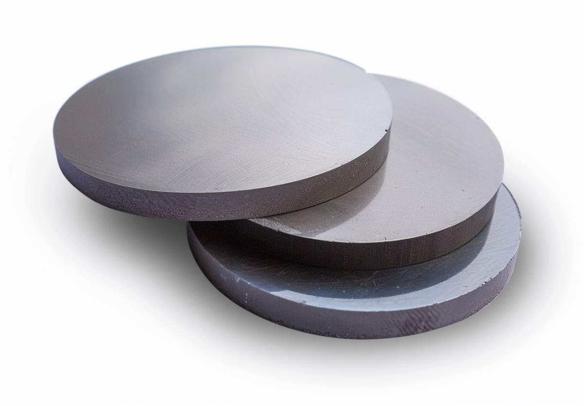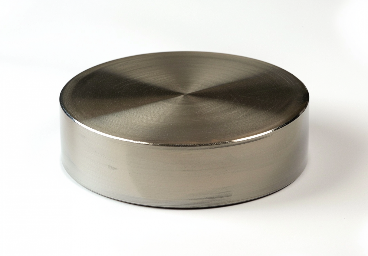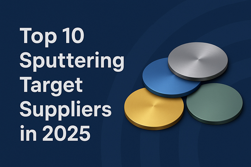
Sputtering targets are a critical instrument utilized by most industries, notably in semiconductor, photovoltaic, and electronics manufacturing via thin-film deposition processes. As more advanced materials are in demand, several companies have distinguished themselves as industry leaders for the production and provision of high-quality sputtering targets. In this article, we have a closer look at the top 10 suppliers of sputtering targets in 2025 based on their products, services, and global presence.
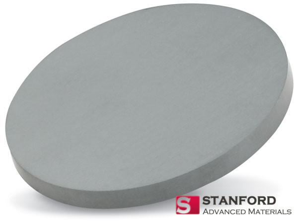
1. Stanford Advanced Materials (SAM)
Year Founded: 1994
Headquarter: Santa Ana, California, USA
Principal Products: High-purity sputtering targets, precious metal, evaporation materials, target recycling service.
Industry Served: Semiconductor, aerospace, medical, energy, material science.
Stanford Advanced Materials (SAM) has developed a good niche in the sputtering target industry. It sells a wide range of high-purity sputtering targets employed in thin-film deposition processes. On the basis of quality control and product range, SAM is an industry leader for those industries requiring advanced materials, particularly in the aerospace and semiconductor industries.
2. Plasmaterials, Inc.
Founded: 1987
Headquarters: Livermore, California, USA
Key Products: Custom sputtering targets, evaporation materials, target plates, plasma spraying.
Industries Served: Thin-film applications, semiconductor, coatings, research and development.
Plasmaterials is a front-runner firm in the thin-film deposition market using custom sputtering targets and evaporation materials. Plasmaterials is strong on providing high-purity products to meet the needs of semiconductor, optics, and coating industries.
3. Kurt J. Lesker Company
Founded: 1954
Headquarters: Jefferson Hills, Pennsylvania, USA
Major Products: Metal, alloy, ceramic, and compound sputtering targets.
Served Industries: Semiconductor, optics, electronics, thin-film deposition.
Kurt J. Lesker Company is an established business company in the sputtering target market. The company has a large range of sputtering targets like metals, alloys, and ceramics and caters to different industries from semiconductor manufacturing to optics. Kurt J. Lesker has a broad product line and its commitment to high standards.
4. MSE Supplies LLC
Founded: 2014
Head Office: Tucson, Arizona, USA
Main Products: Metal, alloy, ceramic sputtering targets, custom targets, copper targets.
Business Sectors Served: Laboratory research, thin-film deposition, engineering.
MSE Supplies LLC provides high-quality sputtering targets that are suitable for scientific research and engineering applications. The company is distinguished by the fact that it has the ability to offer custom sputtering targets that meet the particular needs of different industries and research institutions.
5. SCI Engineered Materials
Founded: 1998
Head Office: Columbus, Ohio, USA
Key Products: Metal and ceramic sputtering targets, evaporation materials, target recycling services.
Industries Served: Solar, semiconductor, electronics, high-tech industry.
SCI Engineered Materials is a trusted provider of sputtering targets and has a strong track record of offering niche-level products in high-tech industries, including solar energy and semiconductor processing. Aside from its main business, the company also provides target recycling services, building a green component to its business.
6. Admat Inc.
Founded: 1997
Headquarters: Norristown, Pennsylvania, USA
Key Products: Refractory metal targets (molybdenum, tantalum, rhenium).
Industries Served: High-temperature uses, optoelectronics, electronics.
Admat Inc. involves refractory metals and their alloys like molybdenum, tantalum, and rhenium. They find wide usage in high-temperature uses as well as optoelectronics. The company’s focus on high-purity, high-performance material positions it as a vital supplier in specialty markets.
7. Goodfellow
Established: 1989
Headquarters: Coraopolis, Pennsylvania, USA
Key Products: A wide range of materials, including sputtering targets, metals, alloys, ceramics.
Industries Supplied: Aerospace, research and development, electronics.
Goodfellow stocks over 70,000 materials, including a very wide variety of sputtering targets. The company’s extensive product range is best suited for industries and scientists who need exotic materials for thin-film deposition and other high-technology applications.
8. Vacuum Engineering & Materials (VEM)
Founded: 1986
Headquarters: Santa Clara, California, USA
Principal Products: Alloy targets, metal targets (copper, gold, aluminum), ITO targets.
Industries Supplied: Energy, electronics, semiconductor.
Vacuum Engineering & Materials (VEM) is a prominent manufacturer of sputtering targets, specializing in metal and alloy targets applicable in thin-film applications. VEM products play an important role in semiconductor materials and electronics production, where accuracy and material purity are highly valued.
9. Mitsui Mining & Smelting Co., Ltd.
Established: Not listed
Head Office: Tokyo, Japan
Principal Products: Sputtering targets, alloy targets, metal materials.
Market Served: Semiconductor, solar energy, electronic displays.
Mitsui Mining & Smelting is a reputable sputtering target supplier with its main markets in the semiconductor, solar energy, and electronic display sectors. As a reliability-first company with high-quality products, Mitsui remains a dominant player in the sputtering target market in Japan and worldwide.
10. Materion
Established: 1931
Headquarters: Buckingham, Ohio, USA
Principal Products: High-purity sputtering targets, metal, alloy, and ceramic material.
Markets Served: Semiconductor, energy, optics.
Materion is a global leader in manufacturing high-purity sputtering targets. It supplies products across industries, from semiconductor manufacturing to power generation and optics. Materion’s focus on precision and high-quality material assures it as a go-to supplier for advanced applications.
Conclusion
The sputtering target industry is propelled by innovation, purity levels, and customized solutions to meet the complex needs of modern manufacturing. Each of the aforementioned companies is the dominant supplier in 2025, each of which brings something unique to semiconductor, energy, and advanced materials fabrication. For high-purity material, customized soluations, or recycling solutions, these companies are consistently shaping the future of thin-film deposition and advanced technology development.
As industries evolve, it’s likely that we’ll see further specialization and innovation, with companies like Stanford Advanced Materials leading the charge in providing comprehensive, high-quality solutions to meet the growing demands of global markets.
Reference:
1. Sputtering Targets Manufacturers and Suppliers in the USA and Canada. Thomas. https://www.thomasnet.com/suppliers/usa/sputtering-targets-83875302
2. (n.d.). 14 Sputtering Targets Manufacturers in 2025. Metoree. https://us.metoree.com/categories/100129/
3. Top Sputtering Target Manufacturers. Ensun. https://ensun.io/search/sputtering-target