Introduction
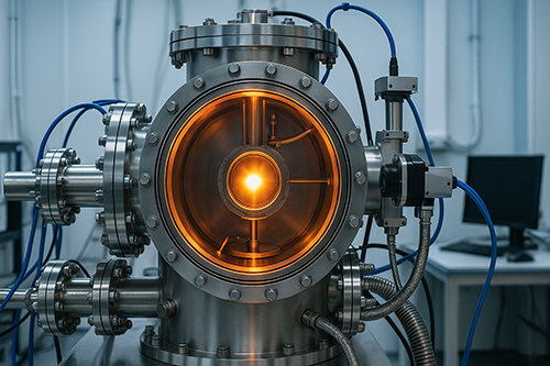
Physical vapor deposition is a trusted method used to apply thin films or coatings on a variety of surfaces. The process works by vaporizing a solid material and letting it settle as a thin, uniform layer on a substrate. People in electronics, optics, and materials science have relied on this technique for years. It allows for a high level of control over how thick the film is and what its composition will be. In everyday terms, it is like the careful painting of a surface at a microscopic level.
To understand the fundamentals of PVD, you can start by exploring the article “What is Physical Vapor Deposition (PVD)?” which offers a comprehensive overview of the process and its significance.
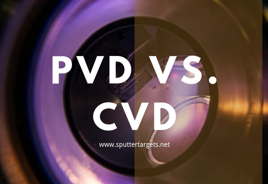
The Basics of Physical Vapor Deposition: How It Works
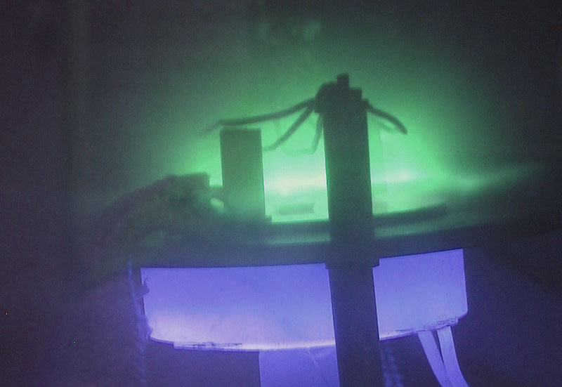
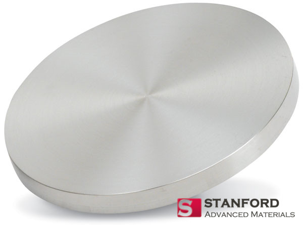
At its core, physical vapor deposition relies on vaporizing a solid material inside a vacuum chamber. The vacuum prevents unwanted particles from getting in the way. There are two main methods. One is evaporation. Here, the material is heated until it turns into vapor. The vapor moves until it meets the cooler substrate, where it then condenses into a thin layer. The other commonly used method is sputtering. In sputtering, a gas such as argon is energized and these energetic ions knock atoms out of a target material. These dislodged atoms travel through the chamber and settle on the substrate.
These processes are simple in theory but require careful management. The temperature, vacuum level, and the rate of deposition must be well-controlled to achieve a uniform layer. Even slight changes can result in a coating that is not smooth or does not cover the substrate completely. I remember working on projects where a small error in the control settings meant we had to start over. This attention to detail is one of the hallmarks of physical vapor deposition techniques.
For a more detailed explanation of the different PVD methods, check out this article.
Key Applications of Physical Vapor Deposition Technology
Physical vapor deposition is used in many practical fields. Let’s look at a few examples:
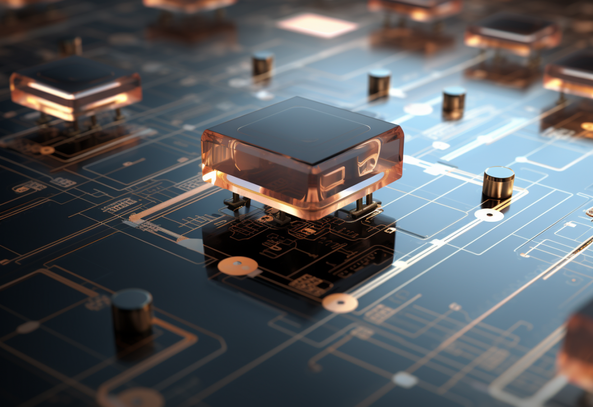
- Semiconductors: In making electronic chips, thin films are essential. A uniform coating allows microcircuits to work properly without interference from impurities or defects. The high level of control in physical vapor deposition ensures that those films meet the strict requirements of modern electronics.
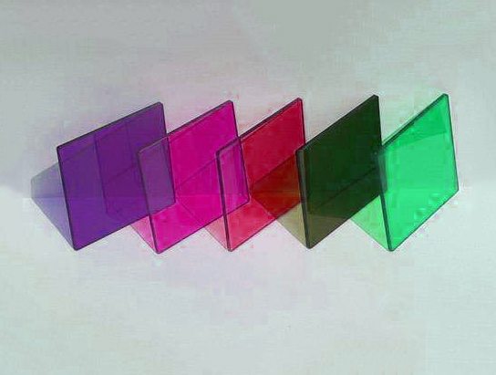
- Optical Coatings: Eyeglasses, camera lenses, and mirrors often benefit from thin optical coatings. A PVD coating can give these surfaces the right amount of reflectivity or help reduce glare. The result is clearer images and better performance in devices that require precise light manipulation.
- Wear and Corrosion Resistance: Think about the coating on tools or machine parts that face daily wear. A thin layer deposited with these techniques can dramatically increase the component’s lifespan. Even simple items that see heavy use, such as engine parts or industrial drill bits, can gain improved hardness and resistance to corrosion. In several cases in my early work, applying such a protective coating proved to be the turning point for durability in harsh operating environments.
The method’s adaptability is one of its greatest strengths. Small electronics or large machine parts both benefit from this controlled layering. This makes physical vapor deposition a practical choice for many situations.
Challenges and Future Trends in Physical Vapor Deposition Technology
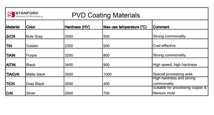
Like many advanced processes, physical vapor deposition has its challenges. One of the biggest issues is achieving a uniform coating over complex shapes. It is easier to coat flat surfaces than parts with many curves and edges. Controlling the deposition rate is another area that requires attention. Sometimes, the cost of high-grade vacuum equipment can also be a concern, especially in smaller applications.
Yet, progress continues steadily. Recently, techniques that involve heated substrates, sometimes referred to as hot sputtering, have shown promising improvements. There are trials with hybrid methods that combine steps from both evaporation and sputtering. These advancements can lead to faster production times and coatings that are even more consistent. In my long career, I have seen many processes evolve, and physical vapor deposition is no exception. The next few years should bring innovations that make the method more accessible while also improving quality.
To stay updated on the latest trends and breakthroughs in PVD technology, refer to the article “Emerging Trends in PVD Technology“.
Choosing the Right Coating Method for Your Needs
Selecting the proper physical vapor deposition technique depends on a few facts. First, consider the material you want to coat. For large surfaces where a moderate coating is acceptable, sputtering is often the best choice because it works well over extended areas. On the other hand, if you need a very thin and precise coat on a smaller surface, evaporation might be your preferred method.
Another factor is the environment where the coating will work. For parts exposed to heavy wear or corrosive substances, a thicker, more durable film might be necessary. I recall working on a project that involved coating components for use in harsh chemical environments. A precisely controlled coating made all the difference in how well the parts performed over time.
The final decision will also depend on the equipment available and the overall cost. In many cases, a trial production run can help determine which method is best suited to a given task. Using the appropriate physical vapor deposition process is both an art and a science—a delicate balance between the desired outcome and the practical limitations of the process.
For more detailed guidance on choosing the best PVD method, take a look at “PVD Coating Methods: A 2025 Guide to Types and Selection“, which outlines the various PVD methods and provides a guide to selecting the most suitable technique for your needs.
Conclusion: The Future of Physical Vapor Deposition Technology
Physical vapor deposition shows no sign of slowing down. As industries push for greater performance and durability, this method remains at the forefront of coating technologies. From the semiconductor industry to optical applications and even protective coatings on everyday tools, the process will continue to be refined and improved.
I have seen many techniques evolve over the years, and physical vapor deposition is naturally on the same path. New methods will likely simplify the production process and lower costs while maintaining high standards. For anyone working with materials that need a reliable, high-performance coating, understanding these processes is a step in the right direction.
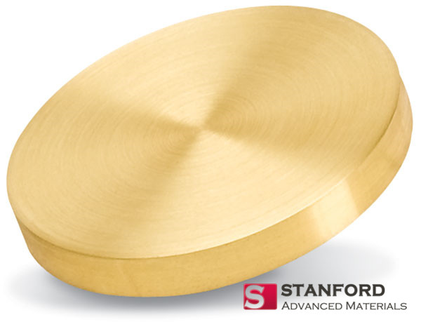
For those looking to source quality physical vapor deposition coatings and related materials, you can rely on Stanford Advanced Materials (SAM). Their products have been crafted to meet the demanding needs of a wide range of industries, ensuring that your application receives the care and precision it deserves.