Platinum sputter targets, integral components in diverse industries, contribute significantly to technological advancements and scientific progress. In this comprehensive exploration, we delve into the wide-ranging applications of platinum sputter targets, illuminating their pivotal role in shaping various sectors.
Semiconductor Industry:
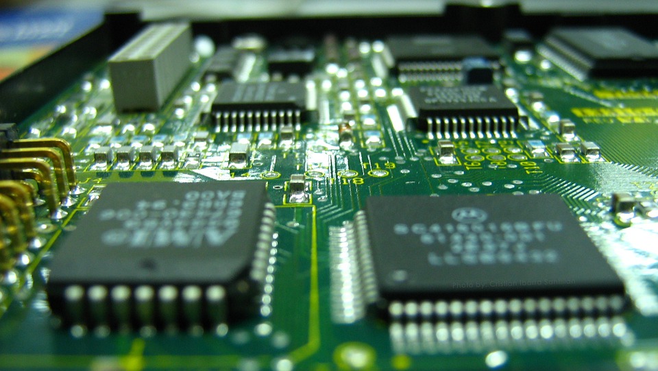
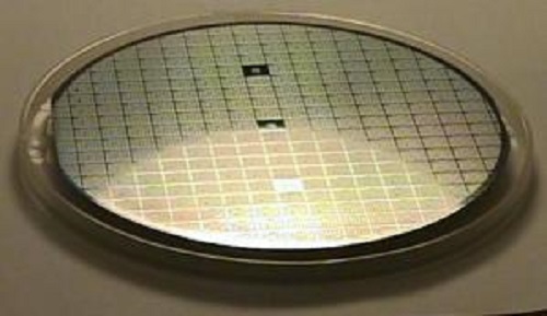
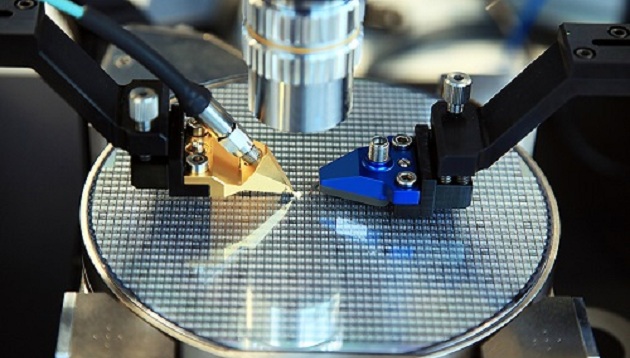
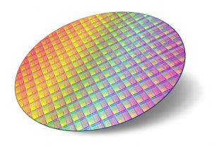
The semiconductor industry heavily relies on platinum sputter targets for the fabrication of integrated circuits, which are the backbone of electronic devices. These targets play a crucial role in the physical vapor deposition process, facilitating the deposition of thin platinum films onto semiconductor wafers. The resulting thin films enhance the performance and miniaturization of transistors and capacitors, contributing to the relentless evolution of semiconductor technology.
Platinum’s remarkable conductivity and stability make it an ideal material for creating thin films that ensure efficient electron flow within semiconductor devices. The precision offered by platinum sputter targets is instrumental in achieving the fine details required for intricate electronic components.
Optical Coatings and Thin Films:
The optical properties of platinum, characterized by high reflectivity and low absorption, position it as a key player in optical coatings. Platinum sputter targets are employed in processes like magnetron sputtering to deposit thin films on optical surfaces. These thin films significantly enhance the reflective properties of mirrors and coatings, making them indispensable in optical devices, telescopes, and lenses.
Beyond reflectivity, platinum’s resilience allows these thin films to endure harsh environmental conditions, ensuring the longevity and sustained performance of optical components.

Biomedical Implants and Devices:
Platinum’s biocompatibility and corrosion resistance make it a preferred material in the biomedical field. Platinum sputter targets are instrumental in depositing thin films on medical implants and devices, enhancing biocompatibility, preventing corrosion, and improving overall device performance and safety.
Consider platinum-coated stents used in cardiovascular procedures, where the thin platinum film ensures compatibility with the human body, reducing the risk of adverse reactions and enhancing the device’s effectiveness.
Catalysis and Sensors:
Platinum’s catalytic prowess places it at the forefront of catalysis and sensor technologies. Platinum sputter targets play a crucial role in creating nanostructured platinum films, elevating their catalytic activity. These nanostructured films find applications in fuel cells, where they facilitate the conversion of chemical energy into electrical energy.
In the realm of sensors, platinum-thin films contribute to the development of highly sensitive and selective sensors. Gas sensors benefit from the conductivity and stability of platinum thin films, enabling precise detection of gases in diverse environments for applications in environmental monitoring, industrial safety, and healthcare.
Flexible Electronics:
The flexibility and durability of platinum sputter targets position them prominently in the realm of flexible electronics. As demand surges for flexible displays, wearable devices, and bendable electronics, platinum thin films, deposited using platinum sputter targets, play a pivotal role in creating conductive and reliable components.
Platinum’s ability to maintain electrical properties under mechanical stress renders it an ideal material for flexible electronic applications. Platinum sputter targets ensure the deposition of thin films that guarantee the longevity and robustness of flexible electronic devices.
Further Reading: Everything You Need to Know About Platinum Sputter Targets
Advancements in Research and Development:
Platinum sputter targets serve as cornerstones in research and development activities, providing a platform for exploring new materials and applications. Materials scientists and researchers leverage platinum thin films to experiment with innovative combinations and structures, pushing the boundaries of achievable feats across scientific disciplines.
Emerging technologies like quantum computing and advanced sensors often rely on platinum thin films as integral components. The precision afforded by platinum sputter targets contributes to the development of devices boasting superior electrical conductivity, magnetic properties, and resistance to environmental factors.
Environmental Considerations and Sustainable Practices:
The use of platinum sputter targets also aligns with environmental considerations and sustainable practices. Recycling platinum from used sputtering targets and electronic waste is gaining attention as a sustainable practice. Efficient recycling processes reduce the environmental impact of platinum extraction and address economic challenges associated with the scarcity of this precious metal.
Global Impact and Collaboration:
The applications of platinum sputter targets extend globally, with research and collaboration fostering advancements on an international scale. International collaboration in materials science and engineering accelerates progress in platinum-sputtering technology. Researchers from different countries contribute diverse perspectives and expertise, leading to breakthroughs that benefit a wide range of industries.
Industrial partnerships further amplify the impact of platinum sputter targets. Collaboration between research institutions and industries facilitates the development of customized platinum thin film solutions tailored to specific industrial requirements, promoting the seamless integration of this technology into various sectors.
Conclusion:
In conclusion, the applications of platinum sputter targets are extensive and influential across multiple industries. From their indispensable role in semiconductor manufacturing to their contributions to optical coatings, biomedical devices, catalysis, and flexible electronics, platinum sputter targets continue to be at the forefront of driving innovation.
The unique properties of platinum, coupled with the precision enabled by sputtering processes, make platinum sputter targets irreplaceable in creating high-quality thin films. As technology advances and new applications emerge, the versatility of platinum sputter targets ensures their sustained significance in shaping the future of various technological fields.
The evolving applications, optimization strategies, and global impact of platinum sputter targets underscore their pivotal role in the ever-expanding realm of thin-film technologies. As we look forward, the journey of platinum sputtering continues, promising further breakthroughs and transformative applications that will shape the future of multiple industries.