A short analysis of sputtering targets for semiconductor application

Semiconductors have high requirements for the quality and purity of the sputtering materials, which explains why the price of anelva  targets is relatively high.

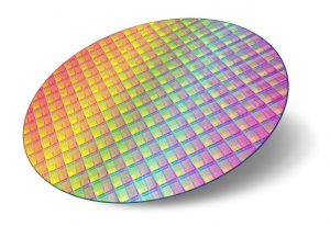
Undoubtedly, sputtering targets are the most important raw materials in current semiconductor manufacturing processes. Their quality and purity play a key role in the subsequent production quality of the semiconductor industry chain. And anelva targets refer to those sputtering targets used in the semiconductor industry.

Application requirements

Semiconductors have high requirements for the quality and purity of the sputtering materials, which explains why the price of anelva  targets is relatively high. In the semiconductor manufacturing process, if the impurity content of the sputtering target is too high, the formed film cannot achieve the required electrical properties, and it is liable to cause short circuit or damage of the circuit, which will seriously affect the performance of the film.

Therefore, when purchasing semiconductor targets, be sure to find a reliable sputtering targets manufacturers for high-quality & high-purity sputtering targets.

blue computer circuit board closeup , semiconductor industry

Market Size

With the rapid development of terminal applications such as consumer electronics, the market sales of high-purity sputtering targets are expanding.

According to statistics, in 2015, the global high-purity sputtering target market sales reached 9.48 billion US dollars, of which, the semiconductor sputtering target market sales of 1.14 billion US dollars. It is estimated that in the next five years, the market size of the world’s sputtering targets will exceed 16 billion US dollars, and the CAGR (Compound Annual Growth rate) of the high-purity sputtering target market will reach 13%.

According to statistics from WSTS (World Semiconductor Trade Statistics), the global target market is expected to grow at the same rate as 2017 (13%). In 2016, the global sputtering target market capacity was US$11.36 billion, an increase of 20% compared to US$9.48 billion in 2015. It can be inferred that the market size of the global high-purity sputtering target in 2018 is about 14.5 billion US dollars.

Stanford Advanced Materials (SAM) Corporation is a global supplier of sputtering targets such as metals, alloys, oxides and ceramic materials, which are widely used in multiple industries. Please visit https://www.sputtertargets.net/ for more information.

Semiconductor industry: The importance of Anelva target

The sputtering target materials can be divided into metal target (pure metal gold, aluminumtitanium, etc.), alloy target (aluminum-scandium alloy, cobalt-aluminum alloy, aluminum-titanium alloy, etc.) and ceramic compound target (oxides, nitride, silicides, etc.) according to their different chemical compositions; when it comes to different application fields, it can be categorized into semiconductor target, planar display target, solar cell target, and other target materials. Anelva target refers to the sputtering target used in semiconductor industry.

Although the proportion of Anelva target is just about 3% among all the sputtering targets, it cannot be denied that its application in semiconductor chip market is important and irreplaceable. There are generally two kinds of Anelva target: wafer materials and packaging materials. Today we mainly focus on wafer manufacturing materials because they have relatively high technical barriers than the other.

The inner part of the semiconductor is composed of tens of thousands of meters of metal wiring, and the sputtering target material is the key consumption material for making these wiring. In other words, the Anelva target is the core of semiconductor wafer manufacturing. Since the chip is elaborate, it has high requirements for sputtering target material used in the manufacturing process. Generally, the purity of the target material is over 99.999%.

Semiconductor wafers are the basic material for manufacturing chips (as shown below). It is small but complicated. The production of wafer mainly involves 7 kinds of semiconductor materials and chemicals. The most important raw material for semiconductor integrated circuits is silicon, which is widely found in rocks and gravel in the form of silicate or silicon dioxide in nature. The manufacturing process of silicon wafers can be divided into three basic steps: silicon purification, monocrystalline silicon growth, and wafer formation. Apart from silicon, the manufacturing process of 200mm (8-inch) and below wafers is usually mainly made of aluminum, and the manufacture of 300mm (12-inch) wafer mostly uses advanced copper interconnection technology.

Semiconductor wafer

In conclusion, with more extensive use of semiconductor chips, the demand for aluminum, titanium, tantalum and copper, the four mainstream Anelva target, will also increase. There is currently no alternative to these target materials, either technically or economically, so, as I mentioned before,  they are important and irreplaceable.

Please visit https://www.sputtertargets.net/ for more information.