Two Methods for Preparing NiCrSi High Resistance Sputtering Target

NiCrSi high-resistance sputtering targets are mainly used to prepare metal film resistors and metal oxide film high resistance resistors, integrated circuit wiring and sensors. These devices are very important in electronic computers, communication instruments, and electronic switches. Due to its excellent performance, resistors made from NiCrSi high-resistance sputtering targets have gradually become a new generation of universal resistors that replace carbon film resistors. Here are two methods for preparing NiCrSi high-resistance sputtering targets.

Adding rare earth metals to improve the target performance

Raw materials: chromium and nickel with an elemental purity greater than 99.5%; silicon with an elemental purity greater than 99.9%; rare earth metals with a mixture purity greater than 98%.

  • Step 1: Smelt Ni, Cr and a small amount of Si into an intermediate NiCrSi alloy. The voltage during the melting of the electric arc furnace is 20V, the current is 500~600A, and the time is 2~5min.
  • Step 2: Place the prepared intermediate NiCrSi alloy was in the bottom of the feeder in a vacuum induction melting furnace. Add the refractory Si material after the intermediate alloy is melted. The vacuum degree during vacuum induction melting is 2 × 10 -2 torr, the power is 35 kW, and the time is 1 h.
  • Step 3: Refining. The power is 20 kW and the time is 30 min.
  • Step 4: Add the rare earth metal in the refining stage. Stir the solution is uniformly by electromagnetic induction and inject it into the investment mold. After the mold is cooled, release the mold to obtain the casting mold.
  • Step 5: Heat treat and machine the target casting. The heat treatment process has a temperature of 800 ° C and a time of 2 h.

Adding titanium to improve the target performance

Raw materials: chromium and nickel with an elemental purity greater than 99.5%; silicon with an elemental purity greater than 99.9%; titanium with an elemental purity greater than 99.5%.

  • Step 1: Use a corundum-graphite-magnesia composite intermediate frequency vacuum induction furnace. Place the prepared materials in a corundum crucible and smelt them under a vacuum of 1×10⁻² torr. The melting temperature is 1,500 to 1,550 ° C, the time 1 h, the power of the medium frequency induction furnace is 10~40kW, and the voltage and current of the induction coil are 100~400V and 200~380A respectively.
  • Step 2: Set a casting tube in the mold shell and extend the nozzle to the bottom surface of the mold shell. Then bake the mold shell to reach 650-700 ° C for casting. After that, cool the mold shell slowly to 850-800 ° C and kept the temperature for 1 h. Then cool it to the room temperature.

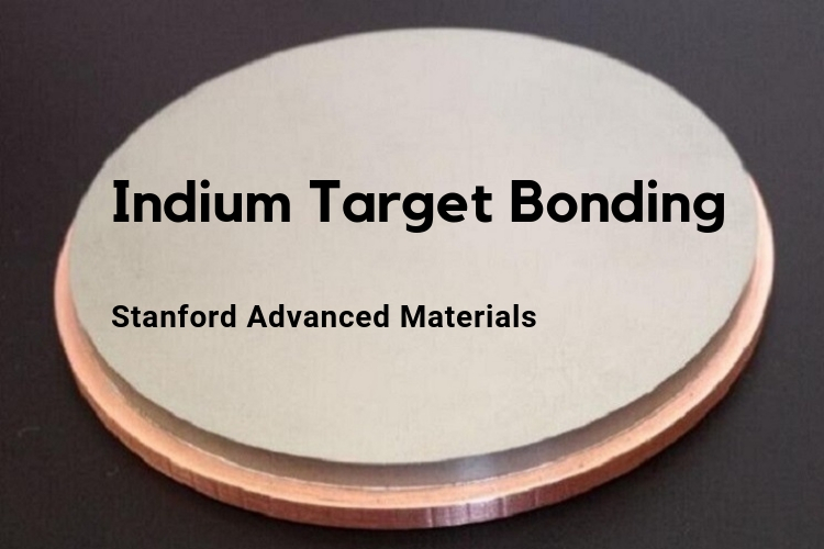
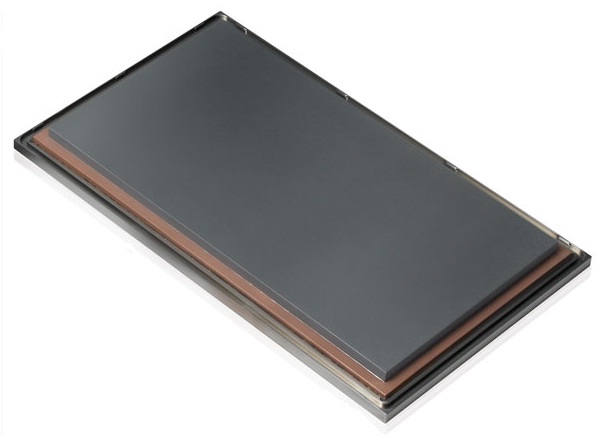
Target Bonding for NiCrSi Target

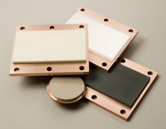
To increase the strength of the target, the NiCrSi target requires a copper plate to be soldered on the back side. The shape and size of the copper plate are the same as the target, and the thickness is 1~3mm. The target and the copper plate are welded firmly by indium bonding or elastomeric bonding, and the soldering temperature is 250 to 270 ° C for 4 hours.

Target Bonding
Target Bonding

Please visit https://www.sputtertargets.net/ for more information.

Year in Review: 2018 Top Posts Collection

Happy New Year in 2019! We are very happy with your company and encouragement that push us to insist on updating every week. On the occasion of the arrival of 2019, let us summarize the Top Posts in 2018 for you.

Metal History

“Metal History” is a popular column we have opened this year, aiming at introducing the discovery of different kinds of metals. Among them, the Top 3 posts in this column are as follows:

How was titanium discovered? | History of Titanium

Titanium is a metal element that is known as “space metal” because of its light weight, high strength and good corrosion resistance. The most common compound of titanium is titanium dioxide, and other compounds include titanium tetrachloride and titanium trichloride. Click the title of the article to know more.

Discovery and development of tungsten | History of Tungsten

The history of tungsten dates back to the 17th century. At that time, miners in the Erzgebirge Mountains of Saxony, Germany, noticed that some of the ore would interfere with the reduction of cassiterite and produce slag. The miners gave the mines some German nicknames: “wolfert” and “wolfrahm”. Click the title of the article to know more.

How was cerium discovered? | History of Cerium

Cerium is the most abundant rare earth elements. It is a silvery gray active metal, whose powder is easily oxidized in the air and soluble in acid. Cerium has been widely used in the automotive industry as a catalyst to reduce emission, and in glass industry as glass polishing materials. Cerium sputtering target is an important material in optical coating. Click the title of the article to know more. Click the title of the article to know more.

Metal Materials Application

Apart from history, we also introduce the multiple applications of these metal materials. Among them, the Top 3 posts in this column are as follows:

Molybdenum Target Mammography Detection

At present, molybdenum target mammography is considered the recommended breast screening examinations for women’s breast cancer, one of the major causes of deaths among women, affects about 12% of women around the world. Click the title of the article to know more.

Application of titanium and titanium alloys in medical field

Titanium is an ideal medical metal material and can be used as an implant for the human body. Titanium alloy has been widely used in the medical field and has become the material of choice for medical products. Click the title of the article to know more.

A short analysis of sputtering targets for semiconductor application

Semiconductors have high requirements for the quality and purity of the sputtering materials, which explains why the price of anelva targets is relatively high. Click the title of the article to know more.

Sputtering Targets

Sputtering Target is the consistent keyword of our website, and thus we have shared many useful information about some specific type of sputtering targets. Our intention is to help you better understand these materials—their properties, applications, developing prospect and so on. And the followings are the posts you really have to read. Among them, the Top 3 posts in this column are as follows:

PVD vs. CVD: What’s the difference?

In recent years, physical vapor deposition (PVD) and chemical vapor deposition (PVD) have wide applications in various industries to increase the hardness of tools and molds or apply beautiful colors to the products. Thus these two methods are considered as the most attractive surface coating technologies. Click the title of the article to know more.

What is the Indium Bonding for Sputtering Target?

The term “indium bonding” in thin film coating industry, simply speaking, refers to bond two (or more) sputtering targets with indium (In), or one (or more) with indium plate together. Click the title of the article to know more.

What is Target Poisoning in Sputtering Deposition?

At some stage in the sputtering deposition, positive ions are continuously amassed on the surface of the sputtering target. Due to the fact that those fantastic ions aren’t neutralized, the negative bias of the target surface gradually decreases, and progressively the normal operation can not be completed. This is the target poisoning phenomenon. Click the title of the article to know more.

Glad you are part of SAM’s 2018. Next year, please continue following us and we promise to give you more valuable information! Also, you can visit our official website https://www.sputtertargets.net/ for more information.

Copper Sulfide Sputtering Targets Are The Best Sputtering Materials

Sputtering is a thin film deposition process in the modern technology world of CDs, semiconductors, disk drives and optical devices industries. Sputtering is the process at an atomic level, where the atoms are automatically sputtered out from the sputtering materials and then be deposited on another substrate, such as a solar panel, semiconductor wafer or optical device. It is an effect of the severe bombard of the high energy particles on the target.

In general, sputtering occurs only when kinetic energy is said to be bombarding particles at very high speeds, which is much higher than a normal thermal energy. At the atomic level, this makes thin film deposition more precise and accurate than that by melting the source material using conventional thermal energy.

Copper Sulfide is the best material for Sputtering Targets. It can be molded into the shape of Plates, Discs, Step Targets, Column Targets and Custom-made. Copper Sulfide is a combination of two materials—Copper and Sulphur. The chemical name of the product is CuS, which offers you the Copper Sulfide product with more than 99 percent purity.


Copper
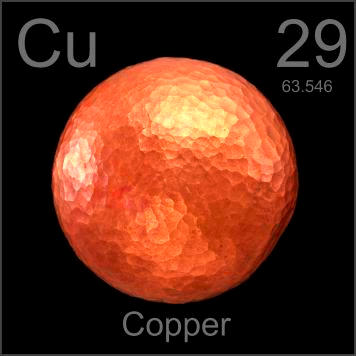
Cyprus is the original source material for the chemical element Copper. The people of Middle East initially discovered it in 9000 BC. “Cu” is the canonical chemical symbol of copper.


Sulfur
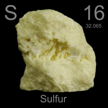
Whereas Sulfur, otherwise known as sulphur, is first introduced in 2000 BC and discovered by Chinese and Indians. It is a chemical name originated from the Sanskrit word ‘sulvere’, and the Latin ‘sulfurium’. Both names are for sulfur.


Copper Sulfide metal discs and plates are highly adhesive and resistant against oxidation and corrosion. Using Copper Sulfide sputtering targets to deposit thin films will not produce highly reflective and extremely conductive films, but can also extensively increase the efficiency of the source energy.

So to achieve the desired noticeable result in a sputtering deposition, the built-up process used to fabricate the Sputtering Targets should be critical. A Copper Sulfide targeted material will give the best result. However, material like only an element, alloys, mixture of elements, or perhaps a compound can be used for the purposes.

For more information about sputtering targets, please visit http://www.sputtertargets.net/.

What is the Indium Bonding for Sputtering Target?

Read more: What Is Indium Bonding for Sputtering Target?

The term “indium bonding” in the thin film coating industry, simply speaking, refers to bonding two (or more) sputtering targets with indium (In), or one (or more) indium plates together.

Indium

Indium can be uniquely used in lower temperature solders, is one of the softest materials. Indium is preferred for target bonding because of its excellent thermal conductivity of all available bonds. In addition, indium is the most efficient material at drawing heat away from the sputtering target. Most materials can be indium bonded and there are just a few exceptions.

Apart from indium bonding, indium is also popular for a variety of uses and purposes, such as creating alloys, photoconductors, and thermistors.

Indium bond

Sputtering targets can be cracked, warped, or damaged due to inadequate cooling, low hardness, or other reasons. From this point of view, although target bonding does generate a fee, it can well protect your target from damage. It is especially true for those less-strong target materials and precious metal materials.

Elastomer is an alternative bonding method that touts a higher temperature capability over the indium bond. Elastomer bonds are recommended when you are consistently melting indium bonds. We also recommend elastomer bonding for low melting point target materials, as well as, temperature-sensitive compounds and targets that have either low density or are especially fragile.

indium target bonding

Indium bonding is preferred in applications where:

Cryogenic stability is needed

Sealing requires high levels of hermeticity

Maximum thermal transfer is required

Bonding to not-metallic surfaces

Flux cannot be used

Backing plates

OFHC Copper Backing Plate is another well-known backing plate. It is frequently used to bond ceramic targets because of its non-magnetism and low coefficient of thermal expansion. This metal has good electrical and thermal characteristics while also being easy to machine, easy to soften, and readily available at a low cost. Copper backing plates can be re-used, with care, 20 or more times.

A molybdenum plate is usually used to substitute copper plate if copper is not appropriate for the application. For instance, the coefficient of expansion for copper is mismatched with some ceramics. And for high-temperature bonding, copper may also oxidize badly or warp. In these conditions, molybdenum is a more suitable material.

SAM Sputter Target

If you are looking for an indium bonding manufacturer, SAM is undoubtedly your best choice. Stanford Advanced Materials is devoted to machining standard backing plates and working together with the Taiwan Bonding Company for providing bonding services. For questions about target bonding materials, methods, and services, please see our listing of frequently asked questions (FAQs).

Related blog: When do you need target bonding?

Requirements of ITO sputtering targets for LCDs

After a long period of development, the quality of liquid crystal displays (LCDs) continues to increase, and the cost continues to decline. This means that LCDs have higher requirements for ITO sputtering targets. Therefore, in order to keep up with the development of LCD, the future development trend of ITO targets is as follows:

Liquid crystal displays
Lower resistivity

In recent years, liquid crystal displays have been moving in a more and more refined direction, and with the upgrade of drivers, a transparent conductive film with lower resistivity is required. Therefore, the resistivity of their raw material—ITO target—is also required to be lowered.

Increase target density

When the target density is low, the surface area for effective sputtering is reduced, and the sputtering speed is also lowered. The high-density target has uniform surface, and can obtain low-resistance film. In addition, the density of the target is also related to its service life, and the high density target generally has a longer life. This means that increasing the density of the target not only improves the film quality, but also reduces the cost of the coating, so it must be the direction for the future development of ITO targets.

Larger size

Now that the LCD screen is getting bigger and bigger, correspondingly, the size of the ITO target has to be larger. However, there are still many problems to be solved in large area coating. In the past, people weld small targets together and splice them to achieve large area coating. But the joints were likely to cause a drop in coating quality. In order to solve this problem, the size of ITO sputtering target is required to be larger in the future. This is also a big challenge for the ITO target industry.

Higher use ratio

Planar targets are still one of the most used types of sputtering targets. But one of the deadliest disadvantage of planar targets is the low use ratio. People may develop other types of ITO target, such as rotatory targets and cylindrical planar targets in the future to increase target utilization.

Please visit https://www.sputtertargets.net/ for more information.

A short analysis of sputtering targets for semiconductor application

Semiconductors have high requirements for the quality and purity of the sputtering materials, which explains why the price of anelva  targets is relatively high.

Undoubtedly, sputtering targets are the most important raw materials in current semiconductor manufacturing processes. Their quality and purity play a key role in the subsequent production quality of the semiconductor industry chain. And anelva targets refer to those sputtering targets used in the semiconductor industry.

Application requirements

Semiconductors have high requirements for the quality and purity of the sputtering materials, which explains why the price of anelva  targets is relatively high. In the semiconductor manufacturing process, if the impurity content of the sputtering target is too high, the formed film cannot achieve the required electrical properties, and it is liable to cause short circuit or damage of the circuit, which will seriously affect the performance of the film.

Therefore, when purchasing semiconductor targets, be sure to find a reliable sputtering targets manufacturers for high-quality & high-purity sputtering targets.

blue computer circuit board closeup , semiconductor industry

Market Size

With the rapid development of terminal applications such as consumer electronics, the market sales of high-purity sputtering targets are expanding.

According to statistics, in 2015, the global high-purity sputtering target market sales reached 9.48 billion US dollars, of which, the semiconductor sputtering target market sales of 1.14 billion US dollars. It is estimated that in the next five years, the market size of the world’s sputtering targets will exceed 16 billion US dollars, and the CAGR (Compound Annual Growth rate) of the high-purity sputtering target market will reach 13%.

According to statistics from WSTS (World Semiconductor Trade Statistics), the global target market is expected to grow at the same rate as 2017 (13%). In 2016, the global sputtering target market capacity was US$11.36 billion, an increase of 20% compared to US$9.48 billion in 2015. It can be inferred that the market size of the global high-purity sputtering target in 2018 is about 14.5 billion US dollars.

Stanford Advanced Materials (SAM) Corporation is a global supplier of sputtering targets such as metals, alloys, oxides and ceramic materials, which are widely used in multiple industries. Please visit https://www.sputtertargets.net/ for more information.

What is Target Poisoning in Sputtering Deposition?

At some stage in the sputtering deposition, positive ions are continuously amassed on the surface of the sputtering target. Due to the fact that those fantastic ions aren’t neutralized, the negative bias of the target surface gradually decreases, and progressively the normal operation can not be completed. This is the target poisoning phenomenon.

The word “poisoning” is normally used to describe the poisoning as a result of the consumption of positive toxic substances via dwelling organisms. However, have you ever heard of target poisoning? Do you already know what it is?

Definition

Despite the fact that the same word is used for “poisoning”, the meaning of target poisoning and human poisoning is completely different. At some stage in the sputtering deposition, positive ions are continuously amassed on the surface of the sputtering target. Due to the fact that those fantastic ions aren’t neutralized, the negative bias of the target surface gradually decreases, and progressively the normal operation can not be completed. This is the target poisoning phenomenon.

target poisoning
target poisoning

Reasons

Target poisoning does not always occur. It is associated with various reasons, of which the following factors are the most significant:

1 There is air leak or water leakage occurs in the vacuum chamber; There are volatile components in the vacuum chamber; The vacuum chamber is not filled with argon, but mixed with air or other gases.

2 The impurity component reacts with the sputtering material to form certain substances, which cover the surface of the sputtering target and affect the film formation speed.

3 There is a change in secondary electron emission, which results in a change of the discharge impedance. Consequently, at the same discharge power, the current and voltage can change substantially as reactive gas is introduced.

Solutions

Luckily, as I mentioned before, the poisoning the the target surface does not always occur, and it can be prevented by the following methods:

1 Ensure that the vacuum chamber is not leaking; Clean the inside of the vacuum chamber regularly to remove volatile components.

2 Irradiate the sputtering target with a medium source or Radio Frequancy (RF) source for one to two hours.

3 If target poisoning occurs, the sputtering target should be removed and be polished with sandpaper.

Please visit https://www.sputtertargets.net/ for more information.

What should we do when the target is broken?

For most of the time, people consider the purity, and maybe the shape, of the sputtering target when they are purchasing the target materials. But one thing should not be ignored is the target bonding. Well, you think it unnecessary and costly? Then just think about what to do when your target is broken.broken target

Target bonding is necessary

Maybe you can use a copper plate to stick the broken pieces of the target and then polish the target so that the broken areas have minimum exposure to plasma. The second step is very important because the power would suddenly breakdown to zero when plasma strike to broken area of target. And obviously, the film quality will be affected if breakdown is frequent. Although it may help solve the problem when the target is broken, it is still a remedial measure. To avoid target from breaking, you need to give a target bonding service to the target. It is necessary for those brittle targets, and is not expensive compared with the losses of the broken target.

Continue reading “What should we do when the target is broken?”

What is Magnesium Fluoride?

Chemical Formula of Magnesium Fluoride

SAM®Magnesium fluoride is an inorganic compound with the formula MgF2, which is a white, fluorescent crystal. It is insoluble in water and alcohol, and soluble in nitric acid. It can be used in ceramics and glass. Magnesium Fluoride is one of the lowest index infrared materials that it is transparent over a wide range of wavelengths, thus is used for optical elements in both the infrared and ultraviolet. It is resistant to thermal and mechanical shock and is twice as hard as Calcium Fluoride.

Continue reading “What is Magnesium Fluoride?”

How is tantalum used in phones?

We have talked about the Application of Tantalum Target in Thermal Inkjet Print Head and Copper Plating before, which rises your interest on this element. However, most people think thermal inkjet print and copper plating are far away from their life, thus are difficult to understand. So today, SAM sputter targets will talk about something that EVERYONE is familiar with—your mobile phones.

tantalum

Tantalum is a very important element in the electronic industry. And it is widely used in all kinds of electronic devices, such as phones and computers. The main use of tantalum materials in electronic products comes in the creation of tantalum capacitor. Tantalum capacitors have their unique advantages over other capacitors. They do not use electrolytes like ordinary electrolytic capacitors, making them ideal for operation at high temperatures. Solid tantalum capacitors have excellent electronic properties, wide operating temperature range, various forms and excellent volumetric efficiency.

Continue reading “How is tantalum used in phones?”