Introduction
In the ever-evolving field of material science, Physical Vapor Deposition (PVD) stands as a cornerstone technology, enabling the development of high-performance coatings across a myriad of industries. At the heart of this technology lies a diverse array of materials, each selected for its unique properties to meet specific application demands. From the reflective surfaces of optical devices to the durable exteriors of aerospace components, the choice of PVD materials directly influences the functionality and efficiency of the final product. This article delves into four pivotal categories of PVD materials—sputtering targets, evaporation materials, inorganic chemicals, and specialized PVD materials—exploring their roles, properties, and the customization options that tailor them to their respective applications.
Read more: PVD Thin Film Deposition Materials List
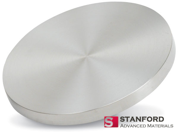
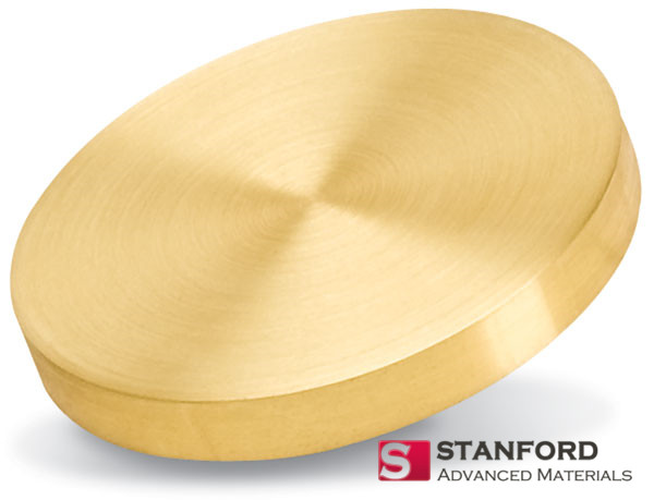
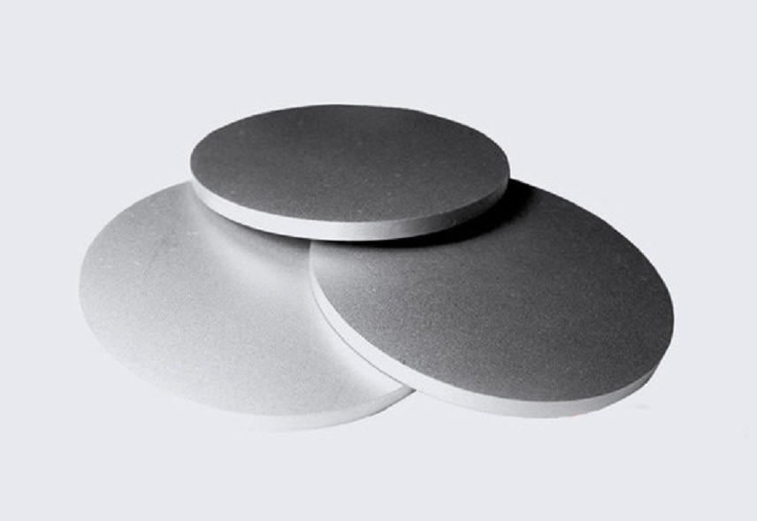
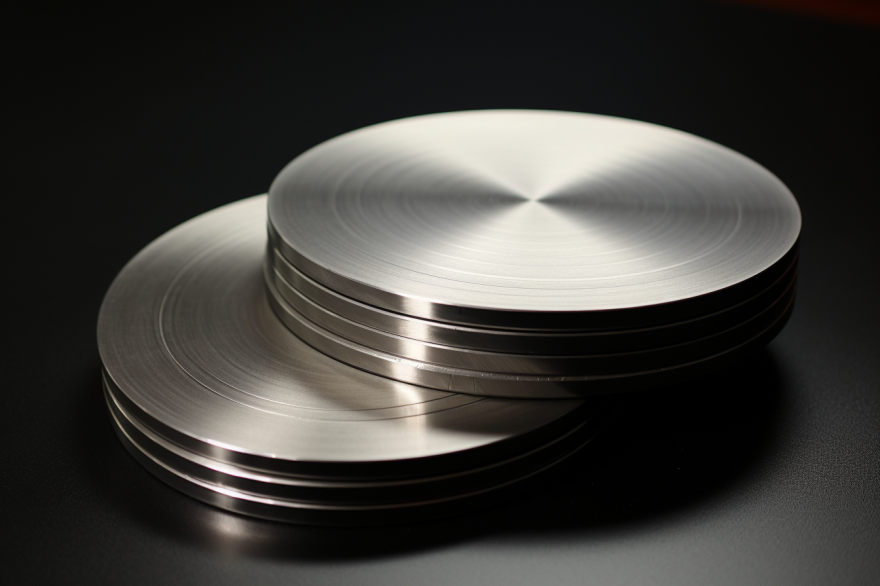
Sputtering Targets
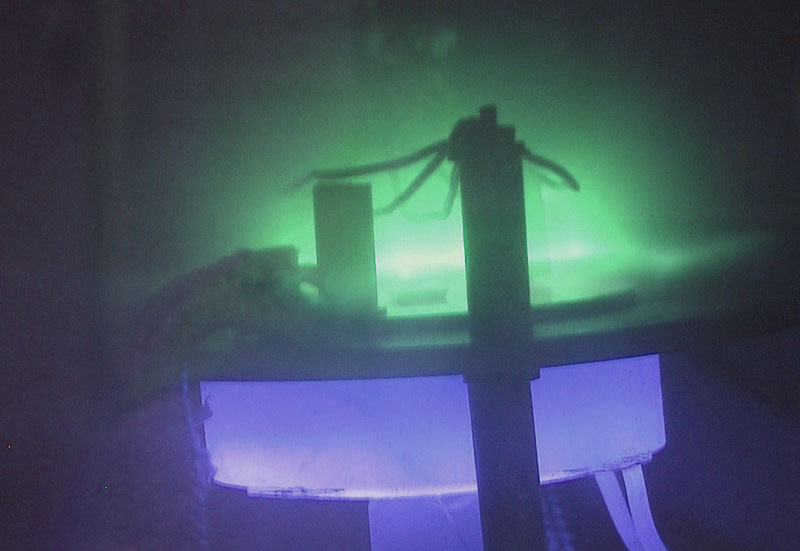
Sputtering targets play a pivotal role in the Physical Vapor Deposition (PVD) process, serving as the source material for thin film coatings. This technique involves bombarding a solid target with high-energy ions, causing atoms to be ejected and deposited onto a substrate, forming a thin film. The choice of target material, such as gold for its unparalleled electrical conductivity or chromium for its exceptional corrosion resistance, is crucial for achieving the desired properties of the final coating.
The customization of sputtering targets is a critical factor in optimizing the PVD process. By tailoring the shape, size, and composition of the target, manufacturers can ensure efficient and uniform deposition, significantly enhancing the performance of the coating. This adaptability allows for a high degree of control over the film’s thickness, composition, and microstructure, meeting the precise requirements of various applications.
Advancements in sputtering technology continue to broaden the range of applications for sputtering targets. From enhancing the durability of aerospace components to improving the efficiency of solar panels, the applications of sputtering targets are expanding into new industries. These advancements not only demonstrate the versatility of sputtering as a deposition method but also underscore the importance of continuous innovation in target material development to meet the evolving needs of technology and industry.
Evaporation Materials
In the realm of Physical Vapor Deposition (PVD), evaporation materials hold a distinct place due to their role in creating thin films through the process of material vaporization and subsequent condensation on a substrate. This method utilizes materials such as silver, known for its excellent reflective properties, making it indispensable for optical coatings. Similarly, copper, celebrated for its high thermal conductivity, is a prime choice for coatings that demand efficient heat management solutions.
The capability to customize these evaporation materials, including the development of specific alloys like Zinc Tin (Zn/Sn), enables engineers to precisely manipulate the thin film’s properties. This level of control is critical for tailoring the film’s optical characteristics, electrical conductivity, or thermal properties to suit specific application needs. By adjusting the composition, form, and purity of the evaporation material, it’s possible to achieve high-performance coatings with optimized characteristics.
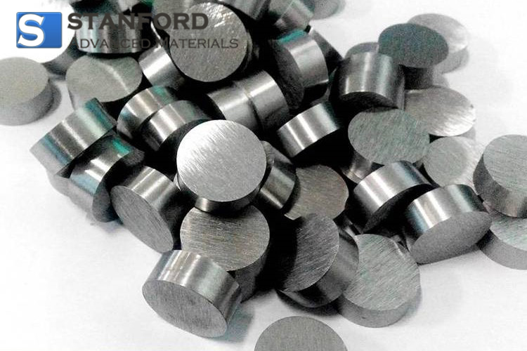
The impact of selecting the right evaporation material extends far beyond the quality of the thin film itself. It influences the efficiency of the deposition process, the durability of the coating, and ultimately, the performance of the end product. For instance, the choice of silver for reflective coatings in high-end optical applications not only enhances the product’s functionality but also its longevity. Similarly, copper’s use in thermal management coatings can significantly improve electronic devices’ performance and reliability by efficiently dissipating heat.
As PVD technologies advance, the possibilities for customizing evaporation materials expand, opening new avenues for innovation in thin-film applications. Whether it’s developing more efficient solar panels or enhancing the durability of electronic displays, the evolution of evaporation materials continues to drive the advancement of coating technologies and the industries they serve.
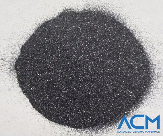
Inorganic Chemicals
Inorganic chemicals serve as fundamental components in the Physical Vapor Deposition (PVD) process, especially when the aim is to achieve specific optical or mechanical properties within thin films. Silicon dioxide (SiO2) and zinc sulfide (ZnS) are exemplary materials in this category, leveraged for their distinct capabilities in enhancing or manipulating light reflection and transmission, critical in optical coatings, and infrared applications, respectively.
The use of inorganic chemicals in PVD processes is highly diversified, thanks to the ability to tailor these materials to precise specifications. Silicon dioxide, for instance, is a staple in creating anti-reflective coatings, significantly reducing unwanted reflections in lenses and display screens. On the other hand, zinc sulfide finds its place in night-vision equipment, exploiting its infrared properties to enhance visibility under low light conditions.
Custom formulation of these chemicals is not uncommon in the industry. Manufacturers often require specific chemical compositions and forms, such as powders or pellets, to achieve optimal application results. This customization ensures that the PVD materials precisely match the intended application’s performance criteria, ranging from enhancing durability to improving efficiency or aesthetic qualities.
Case studies across various sectors demonstrate the effectiveness of inorganic chemicals in specialized coatings. For example, the application of silicon dioxide in the telecommunications industry has enabled the production of more efficient fiber optic cables by minimizing light loss. Similarly, the automotive sector benefits from zinc sulfide-based coatings, enhancing the durability and performance of infrared sensors used in driver-assistance systems.
These examples underscore the critical role of inorganic chemicals in advancing PVD technology and their contribution to the development of innovative products and solutions. The ability to customize these materials to meet exacting standards is a testament to the flexibility and adaptability of PVD processes, paving the way for further advancements in materials science and engineering.
Specialized PVD Materials
The category of specialized PVD materials includes advanced compounds such as silicon carbide (SiC) and aluminum nitride (AlN), each selected for its unique set of properties that address specific challenges in harsh environments and high-tech applications. These materials exemplify the innovative edge of PVD technology, offering solutions where traditional materials fall short.
Silicon Carbide (SiC) stands out for its exceptional hardness and thermal conductivity, making it an ideal candidate for protective coatings in environments subjected to extreme wear and high temperatures. Its application spans various industries, from aerospace, where engine components benefit from SiC’s durability and thermal resistance, to electronics, where SiC enhances the longevity and performance of semiconductor devices.
Aluminum Nitride (AlN), with its remarkable electrical insulation properties combined with high thermal conductivity, is particularly valuable in electronic applications. It’s used to fabricate substrates and insulating layers that can efficiently draw heat away from sensitive electronic components, thus preventing overheating and ensuring reliable operation under demanding conditions.
The role of these specialized materials in advancing PVD applications cannot be overstated. They not only provide enhanced performance and durability but also enable the development of technologies that were previously unattainable. For instance, the use of SiC in protective coatings has led to the creation of cutting tools that can operate at higher speeds and temperatures, significantly increasing productivity and reducing downtime.
Looking forward, the potential for new compounds and innovative applications of specialized PVD materials is vast. Ongoing research and development are expected to unveil materials with even greater capabilities, further expanding the horizons of what can be achieved with PVD coatings. Whether it’s developing ultra-resistant coatings for next-generation spacecraft or creating more efficient thermal management solutions for the latest electronics, specialized PVD materials are at the forefront of technological innovation.
Conclusion
The exploration of the four pivotal categories of PVD materials—sputtering targets, evaporation materials, inorganic chemicals, and specialized PVD materials—reveals the depth and breadth of options available for modern coating technologies. Each category offers unique properties that can be tailored to meet the exacting demands of various applications, from enhancing the optical performance of devices to improving the durability of components exposed to extreme conditions.
This diversity not only underscores the versatility of PVD technology but also highlights the importance of material selection in achieving the desired outcomes. Whether it’s choosing the right sputtering target for electrical conductivity or selecting a specialized material for thermal insulation, the success of PVD processes hinges on a deep understanding of material properties and their interactions with specific applications.
Looking ahead, the continued innovation and development of new PVD materials promise to further expand the capabilities of this technology. As industries push for higher performance standards and environmental sustainability, the role of advanced PVD materials will undoubtedly grow, driving new applications and improvements across a wide range of sectors.
For those navigating the complexities of PVD processes, the guidance o
experts and suppliers like Stanford Advanced Materials (SAM) can prove invaluable. SAM’s expertise in providing high-quality PVD materials, coupled with a deep understanding of industry-specific requirements, ensures that clients can make informed decisions, optimizing their processes and products for the challenges of tomorrow.
In conclusion, the role of PVD materials in advancing technological and industrial innovations cannot be overstated. As we continue to explore the potential of these materials, their impact on shaping the future of manufacturing, electronics, aerospace, and beyond is poised to be profound, marking a new era of material science and engineering excellence.