Application and Recycling of Tungsten Metals

Tungsten, a relatively rare and exotic metal, has been widely used in many products in our daily life. Tungsten has the advantages of high melting point, high hardness, excellent corrosion resistance, and good electrical and thermal conductivity. Most of its applications are based on these properties. Tungsten is not cheap because of its scarcity, but the price of tungsten is quite reasonable compared with the prices of other rare and exotic metals.

What are the Applications of Tungsten?

Tungsten is an important alloying element for the aerospace industry and the industrial gas turbine industry, because it can significantly improve the strength, hardness, and wear resistance of steel.

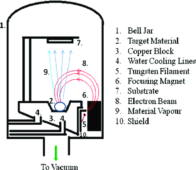
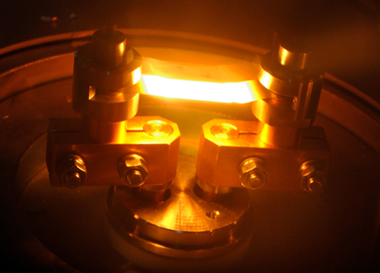
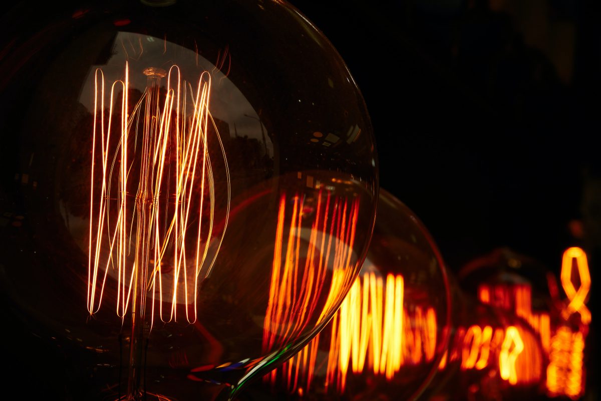
Tungsten filament is used in incandescent bulbs to replace tantalum, which was used many years ago, as an integral part of copper and silver electrical contacts for improved wear resistance.  Tungsten wire can also be used to manufacture direct heating cathodes and grids of electronic oscillation tubes and cathode heaters in various electronic instruments.

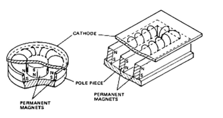
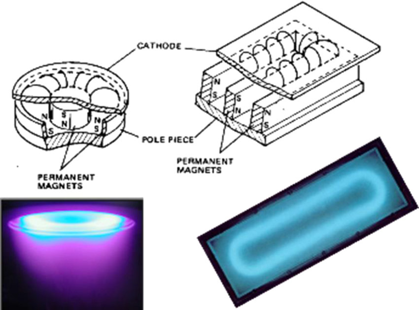
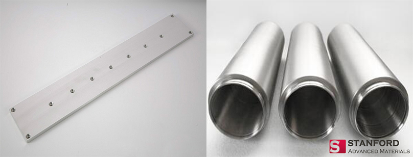
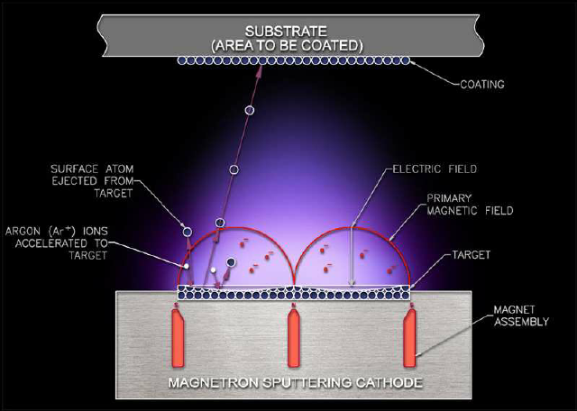
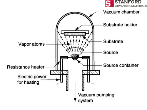
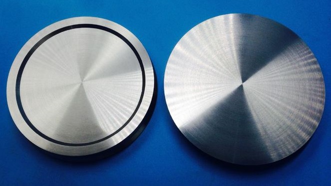
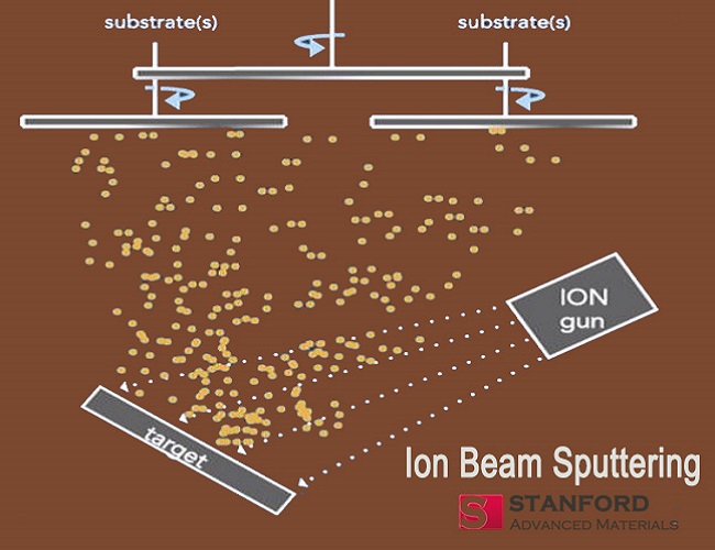
Tungsten sputtering target & Ta evaporation pellets can be used as wear-resistant coatings for mechanical parts, as evaporating filaments for physical vapor deposition (PVD) of aluminum and silver, and as key barrier electrons for barrier coatings in critical electronic devices.

Some of the other applications of Tungsten include the component of chemicals and catalysts, cutting blades, paints, pigments, inks, lubricants, etc.

How to Recycle Tungsten?

Tungsten’s unique properties of heavy weight, high hardness, and high melting point make tungsten waste ideal for recycling. The fact that it is chemically resistant is a key factor in tungsten recycling. Therefore, recycling tungsten-bearing scrap is more popular. The methods of tungsten recycling can be roughly divided into the direct method and the indirect method.

Direct Tungsten Recycling

The direct method means that the tungsten waste is converted into a powder of the same composition by chemical or physical treatment or a combination of both. A typical example of a direct method is a zinc treatment method. This method has many advantages, such as limited energy consumption and chemical waste, as well as low production costs. A disadvantage of this method is the limitation on recycled materials.

Indirect Tungsten Recycling

Indirect methods, such as wet chemical processing, are commonly used in refining processes. This type of recycling has no restrictions on materials, but requires a lot of chemicals and energy.

For more information, please visit https://www.sputtertargets.net/.

Magnetrons & Magnets Used in Magnetron Sputtering

The planar magnetron is an exemplary “diode” mode sputtering cathode with the key expansion of a permanent magnet cluster behind the cathode. This magnet exhibit is organized so that the attractive field on the substance of the target is ordinary to the electric field in a shut way and structures a limit “burrow” which traps electrons close to the surface of the target. This enhances the effectiveness of gas ionization and compels the release plasma, permitting higher presence at the lower gas weight and attaining a higher sputter affidavit rate for Physical Vapor Deposition (PVD) coatings.

Although some distinctive magnetron cathode/target shapes have been utilized in magnetron sputtering processes, the most widely recognized target types are circular and rectangular. Circular magnetrons are all the more regularly found in littler scale “confocal” cluster frameworks or single wafer stations in group instruments. Rectangular Magnetrons are frequently found in bigger scale “in line” frameworks where substrates examine straightly past the focus on some type of carpet lift or transporter.

Color-online-Upper-Illustrations-of-circular-and-rectangular-planar-magnetron
Color-online-Upper-Illustrations-of-circular-and-rectangular-planar-magnetron. Greene, J.. (2017). Review Article: Tracing the recorded history of thin-film sputter deposition: From the 1800s to 2017. Journal of Vacuum Science & Technology A: Vacuum, Surfaces, and Films. 35. 05C204. 10.1116/1.4998940.

Most cathodes – including practically all circular and rectangular ones – have a straightforward concentric magnet design with the middle being one shaft and the edge the inverse. For the circular magnetron, this would be a generally little adjusted magnet in the middle, and an annular ring magnet of the inverse extremity around the outside with a hole in the middle. For the rectangular magnetron, the core one is typically a bar down the long hub (however short of the full length) with a rectangular “wall” of the inverse extremity and the distance around it with a hole in the middle. The crevice is the place the plasma will be, a roundabout ring in the circular magnetron or a lengthened “race track” in the rectangular.

The magnetron works with either an attractive arrangement – the middle could be north and the border might be south, or the other way around. Notwithstanding, in most sputter frameworks, there are various cathodes in reasonably close vicinity to one another, and you don’t need stray north/ south fields structured in the middle of the targets.

Those N/S fields ought to just be on the targets’ confronts, structuring the coveted attractive shafts there. Hence, it is completely attractive to verify all the cathodes in one framework are adjusted the same way, either all north on their borders or all south on their edges. What’s more, for offices with numerous sputter frameworks, it is similarly alluring to make all of them the same so cathodes can securely be traded between the frameworks without agonizing over magnet arrangement.

There are extra contemplations and choices in regard to the magnets. Most target materials are nonmagnetic and in this manner don’t meddle with the obliged attractive field quality. However, in the event that you are sputtering attractive materials, for example, iron or nickel, you will require either higher quality magnets, more slender targets, or both with a specific end goal to abstain from having the surface attractive field adequately shorted out by the attractive target material.

Past that, the magnet’s subtle elements, for example, attractive quality and crevice measurements, might be intended to enhance target material usage or to enhance consistency along the vital pivot of a rectangular target. It is even conceivable to utilize electromagnets rather than perpetual magnets, which can manage the cost of some level of programmable control of the attractive field, yet does, obviously, build many-sided quality and expense.

For more information, please visit https://www.sputtertargets.net/.

How to Judge the Uniformity of PVD film?

PVD, Physical Vapor Deposition, is a general term for a series of coating methods. It includes two main categories: evaporation deposition coating and sputtering deposition coating. To specifictly classify it, there are vacuum ion evaporation, magnetron sputtering, MBE molecular beam epitaxy, sol gel method, etc.

For PVD vacuum coating with different principles, the concept of uniformity will have different meanings with the coating scale and film composition, and the factors affecting uniformity are also different. In general, film uniformity can be understood from the following three aspects.

Uniformity in thickness (roughness)

From the scale of optical films (that is, 1/10 wavelength as a unit, about 100A), vacuum coating can easily control the roughness within 1/10 of the wavelength of visible light, and the uniformity is quite good.

But if it refers to the uniformity on the atomic layer scale (that is to say, to achieve 10A or even 1A surface flatness), the roughness of the film can be good or bad, which is also the main technical content and technical bottleneck in the current vacuum coating.

The thickness uniformity is mainly determined by the following points: 1) the degree of lattice matching between the substrate material and the target material; 2) the surface temperature of the substrate; 3) evaporation power, speed; 4) vacuum degree; 5) coating time, thickness.

Thin film thickness

Uniformity in chemical composition

In thin films, the atomic composition of compounds can easily produce non-uniform properties due to their small size. For example, in the process of preparing SiTiO3 thin films, if the material ratio and environment are not strictly controlled, the components of the prepared surface may not be SiTiO3, but Sr, Ti, and O may exist in other proportions.

The uniformity of the components of the evaporation coating is not easy to guarantee, and the specific factors that can be adjusted are the same as the above, but due to the limitation of the principle, for the non-single component coating, the uniformity of the components of the evaporation coating is not good.

Uniformity of lattice order

This determines whether the film is single crystal, polycrystalline, or amorphous. It is also a hot issue in vacuum coating technology.

For more information, please visit https://www.sputtertargets.net/.

3 Factors of Target Quality Influence Large-area Coating

Most modern buildings have begun to use large areas of glass for lighting, and its biggest advantage is that it can bring us brighter light and a wider view. However, since the heat energy transmitted through the glass is much higher than the surrounding walls, the energy consumption of the entire building increases significantly. In order to solve this problem, people have begun to study and apply large-area Low-E glass.

Low-E glass is commonly used in building construction because of its ability to save energy, control light, and for aesthetics. The sputtering target material is one of the essential components for making low-e glass, so this article will introduce 3 factors of target quality that influence large-area coating of low-E glass.

The shape of the target materials

For large-area coating, commonly used targets include planar targets and rotatory targets according to their shapes. The shape of the target affects the stability and film properties of the magnetron sputtering coating, as well as the utilization rate of the target. Therefore, the coating quality and production efficiency can be improved by changing the shape design of the target, and the cost can be saved.

planar targets and rotatory targets
Planar targets and rotatory targets

Relative density & porosity of the target

The relative density of the target is the ratio of the actual density to the theoretical density. The theoretical density of a single-component target is the crystal density, and the theoretical density of an alloy or compound target is calculated from the theoretical density of each component and its proportion in the alloy or mixture.

If the target material is loose and porous, it will absorb more impurities and moisture, which are the main pollution sources in the coating process. These impurities will hinder the rapid acquisition of high vacuum, easily lead to electrical discharge during the sputtering process, and even burn out the target. Find high-quality target material here: https://www.sputtertargets.net/

Target grain size and crystallographic direction

For targets of the same composition, the one with the smaller grain size has a faster deposition rate. This is mainly due to the fact that grain boundaries are more vulnerable to attack during the sputtering process, and the more grain boundaries, the faster the film formation.

In addition, the grain size also affects the quality of the film formation. For example, in the production process of Low-E glass, NiCr thin-film is used as the protective layer of the infrared reflection layer Ag, and its quality has a great influence on the coating products. Since the extinction coefficient of the NiCr film is relatively large, it is generally plated very thinly (about 3nm). If the grain size is too large and the sputtering time is short, the compactness of the film will be poor, the protective effect of the Ag layer will be reduced, and the coating product will be oxidized and removed.

Conclusion

The shape of the target mainly affects the utilization rate of the target material, and a reasonable size design can improve the utilization rate of the target material and save costs. The smaller the grain size, the faster the coating rate and the better the uniformity. The higher the purity and density, the lower the porosity, the better the quality of the film formation, and the lower the probability of slag removal by discharge.

Electron Beam Deposition for Film Coating

Introduction

Electron beam deposition is a form of physical vapor deposition (PVD) in which the target anode material is bombarded with a stream of electrons generated by a tungsten filament. Electron beam thin film deposition techniques are widely used in R&D as well as in mass production applications.

Electron beam deposition is performed in a vacuum, typically starting the process at levels below 10-5 Torr. Once a suitable vacuum is reached, a tungsten filament in the electron beam source emits a stream of electrons. This electron beam can be generated in various ways, including thermionic emission, field electron emission, or ion arc source, depending on the design of the source and associated power supply.

In all cases, the negatively charged electrons are attracted to the positively charged anode material. The generated electron beam is accelerated to high kinetic energy and directed towards the material to be deposited on the substrate. This energy is converted into heat by interacting with the atoms of the evaporated material.

The purpose of generating a stream of electrons in an electron beam source is to heat the deposited material to a temperature above a vapor pressure threshold at a given background pressure. The vapor stream is then condensed onto the surface of the substrate.

Schematic representation of electron beam evaporation system depicting various parts.
Schematic representation of electron beam evaporation system depicting various parts.. Mohanty, P. & Kabiraj, Debdulal & Mandal, R.K. & Kulriya, Pawan Kumar & Sinha, Ask & Rath, Chandana. (2014). Evidence of room temperature ferromagnetism in argon/oxygen annealed TiO2 thin films deposited by electron beam evaporation technique. Journal of Magnetism and Magnetic Materials. 355. 240–245. 10.1016/j.jmmm.2013.12.025.

Deposition Rate

As with all thermal evaporation systems, the electron beam deposition rate depends on the temperature of the material being deposited and the vapor pressure (physical constant) of that material. For elemental materials, there is a fixed vapor pressure for any particular background pressure (vacuum) and material temperature. However, for alloys or composites, there may be different partial pressures associated with each component.

Compared with Sputter Coating

Unlike sputter deposition, where individual atoms arrive at the substrate surface with very high velocity and momentum, the thermally generated vapor stream arrives at the substrate surface at a considerably lower velocity, but a much greater velocity. In other words, e-beam deposition rates can be orders of magnitude greater than sputter deposition rates, making e-beam coatings very beneficial for high volume production or thick film requirements. One disadvantage, however, is that the material tends to condense directly on the substrate surface due to the different kinetic energy of the arriving species during electron beam evaporation than that of the sputtered species. In contrast, atoms of sputtered materials tend to penetrate several atomic layers (or more) to the substrate surface before losing momentum and then establishing cohesive bonds in nucleation structures and film growth. Thus sputtered films tend to provide better adhesion properties than thermally evaporated materials.

For more information, please visit https://www.sputtertargets.net/.

Evaporation Coating Experiment: Principle, Purpose & Results

Introduction

In recent years, the rapid economic development and the continuous improvement of people’s living standards have led to the continuous emergence of high-tech thin-film products, especially in the field of electronic materials and components. Vacuum coating technology has also gained significant application in this field.

At present, the common film-forming methods include vapor-phase film-forming method, oxidation method, ion implantation method, diffusion method, electroplating method, coating method, liquid-phase growth method, etc. The vapor generation method can be further subdivided into physical vapor deposition, chemical vapor deposition, and discharge polymerization.

Principle

The experiments listed in this article are related to physical vapor deposition coatings. This method is basically carried out under vacuum, so it is called vacuum coating technology.

Vacuum evaporation, sputter coating, and ion plating are commonly referred to as basic physical vapor deposition thin film preparation techniques. The vacuum evaporation coating method is a method in which the evaporation material of a film to be formed in a vaporization chamber is heated in a vacuum chamber, and atoms or molecules are vaporized from the surface to form a vapor stream, which is incident on the surface of the substrate and condensed to form a solid film.

Evaporation Coating

Purposes

  1. To familiarize yourself with the operating procedures and methods obtained by vacuum;
  2. In order to understand the principle and method of evaporation coating;
  3. To learn how to use evaporation coating technology.

Results

(1) Vacuum conditions during evaporation

When the average free path of the vapor molecules in the vacuum vessel is greater than the distance between the evaporation source and the substrate (called the steaming distance), sufficient vacuum conditions are obtained. For this reason, it is necessary to increase the mean free path of the residual gas to reduce the collision probability of the vapor molecules with the residual gas molecules, and to evacuate the vacuum chamber to a high vacuum.

(2) How to choose evaporation source selection

1 It should have good thermal stability, chemical inactivity; the vapor pressure of the heater itself is sufficient to reach the evaporation temperature.

2 Its melting point should be higher than the evaporation temperature of the evaporated material. The heater should have a large enough heat capacity.

3 The mutual melting of the evaporated material and the evaporation source material must be very low, and it is difficult to form an alloy.

4 The material used for the coil-shaped evaporation source is required to have a good wetting with the evaporation material and a large surface tension.

5 For a case where it is difficult to form a filament, or when the surface tension of the evaporation material and the filament evaporation source is small, a boat-shaped evaporation source can be used.

(3) Main physical processes of thermal evaporation coating

1 Using various forms of thermal energy conversion to vaporize or sublimate the coating material into gaseous particles (atoms, molecules or atomic groups) with certain energy (0.1~0.3eV);

2 Gaseous particles are transported to the substrate by a substantially collision-free linear motion;

3 Particles are deposited on the surface of the substrate and agglomerated into a film.

(4) Factors affecting the quality and thickness of vacuum coating

There are many factors affecting the quality and thickness of the vacuum coating, including the degree of vacuum, the shape of the evaporation source, the position of the substrate, and the temperature of the evaporation source. The solid matter has very low evaporation at normal temperature and normal pressure. The higher the degree of vacuum, the easier it is for the molecules of the evaporation source material to scatter away from the surface of the material. The fewer molecules in the vacuum chamber, the lower the probability that the evaporating molecules will collide with the gas molecules, so that the surface of the substrate can be reached unobstructed straight.

For more information, please visit https://www.samaterials.com/.

Study on Preparation Methods of Magnesium Film Materials

Thin-film is a rapidly developing material in the field of modern material science and technology, and there are many methods for its preparation. This article introduces several methods for preparing thin films, focusing on magnetron sputtering and ion beam sputtering deposition, and using magnesium sputtering targets as raw materials to prepare magnesium thin films.

Magnesium is in a diagonal position with lithium in the periodic table of the elements, has similar chemical properties to lithium, and has some electrochemical properties better than lithium, which can meet the needs of power batteries. Magnesium batteries have many advantages such as low cost, non-toxicity, no pollution, stable discharge voltage, high specific energy, high specific power, rich resources, and renewable. However, magnesium batteries have not been widely used. One of the main reasons is that magnesium is severely polarized and corroded in the electrolyte, making it unable to meet the applicable standards and difficult to meet the actual requirements. Research on magnesium thin-film materials can help improve this defect of magnesium batteries.

Principle of magnetron sputtering coating

Sputter deposition is the process whereby particles of sputtering materials are sputtered out and deposited on a substrate to form a film. Since ions are charged particles, we can add magnetic fields to control their speed and behavior. And that’s how its name “magnetron sputtering” comes from.

Under the action of an electric field of several hundred to several thousand electron volts, the plasma is accelerated and obtained sufficient force to bombard the cathode, causing the atoms of the solid sputtering target to be ejected in a typical line-of-sight cosine distribution. These atoms will condense on the surface of the substrate to form a thin film.

Ion beam sputtering coating

Ion beam sputtering (IBS), or ion beam deposition (IBD), is a thin film deposition technology that uses an ion source to deposit a sputtering target onto a substrate to produce the highest quality films with excellent precision. Compared to other PVD technologies, ion beam sputtering is more accurate and can accurately control the thickness of the substrate. As shown below, an IBS system usually includes the ion source, the target material, and the substrate. The ion beam, usually generated by the ion gun, is focused on the sputtering target, and the sputtered target material finally deposits onto the substrate to create a film.

Preparation of magnesium film material

In the preparation of magnesium-thin films, magnetron sputtering is a very good choice. This method has the advantages of high speed, low temperature and low damage. The deposited layer is uniform, dense, has small pinholes, high purity, and has strong adhesion. These advantages are the key to the quality of magnesium films. The selected targets are high-purity powder-pressed magnesium sputtering targets and magnesium alloy sputter targets.

For more information about thin-film coating, please visit https://www.sputtertargets.net/.

Advantages of Sputtering Deposition and Vacuum Evaporation

For all devices, there is a need to go from semiconductor to metal. Thus we need a means to deposit metals, also called film coating. There are currently several methods for depositing metal thin film layers, and many of these techniques for metal deposition can also be used to deposit other materials.

1.) Physical Vapor Deposition (PVD)

2.) Electrochemical techniques

3.) Chemical Vapor Deposition (CVD)

This passage will talk about the advantages of two PVD methods: Sputtering and evaporation.

Sputtering Deposition

magnetron-sputtering-system
Magnetron Sputtering System

The plasma under high pressure is used to “sputter” metal atoms out of the “target”. These high-energy atoms are deposited on a wafer near the sputtering target material. Higher pressures result in better step coverage due to more random angular delivery. The excess energy of the ions also helps increase surface mobility (the movement of atoms on the surface).

Advantages: Better step coverage, less radiation damage than E-beam evaporation, easier to deposit alloys.

Disadvantages: Some plasma damage including implanted argon. Good for ohmics, not Schottky diodes.

Vacuum Evaporation

Evaporation (PVD)
Evaporation (PVD)

Evaporation is based on the concept that there exists a finite “vapor pressure” above any material. The material either sublimes (direct solid to vapor transition) or evaporates (liquid to vapor transition).

Advantages: Highest purity (Good for Schottky contacts) due to low pressures.

Disadvantages: Poor step coverage, forming alloys can be difficult, lower throughput due to low vacuum.

PVD Film Morphology

The three zone model of film deposition as proposed by Movchan and Demchishin

1.) Porous and/or Amorphous —> Results from poor surface mobility =low temperature, low ion energy (low RF power/DC bias or higher pressures=less acceleration between collisions).

2.) “T-zone”: Small grain polycrystalline, dense, smooth and high reflectance (the sweet spot for most metal processes) Results from higher surface mobility =higher temperature or ion energy

3.) Further increases in surface mobility result in columnar grains that have rough surfaces. These rough surfaces lead to poor coverage in later steps.

4.) Still further increases in surface mobility result in large (non-columnar) grains. These grains can be good for diffusion barriers (less grain boundary diffusion due to fewer grains) but pose problems for lithography due to light scatter off of large grains, and tend to be more rigid leading to more failures in electrical lines.

For more information, please visit https://www.sputtertargets.net/.

What are the Uses of Metal Sputtering Targets?

What is the “target”?

The target refers to the target material. They can be used in high-energy laser weapons; different power densities, different output waveforms, and different wavelengths of lasers can have different killing effects when interacting with different targets. Another major use for them is for sputtering in physical film coating.

What is the “sputtering target”?

Magnetron sputtering coating is a new type of physical vapor deposition method, and its advantages in many aspects are quite obvious compared with the earlier evaporation coating method. As a relatively mature technology that has been developed, magnetron sputtering has been applied in many fields. Sputtering targets serve as source materials in magnetron sputtering coatings.

sputtering target in lcd

What are the application areas?

1: Microelectronics field

2: Target for flat panel display

3: Targets for storage technology

Sputtering materials are mainly used in electronics and information industries, such as integrated circuits, information storage, liquid crystal displays, laser memories, electronic control devices, etc.; they can also be used in the field of glass coating; they can also be applied to wear-resistant materials, high temperature corrosion resistance, high-grade decorative products and other industries.

The technological development trend of target materials is closely related to the development trend of thin-film technology in the downstream application industry. As technology in the application industry improves on film products or components, target technology should also change. In recent years, flat panel displays (FPDs) have largely replaced the market for computer monitors and televisions, which are mainly cathode ray tubes (CRTs), and will greatly increase the technical and market demand for ITO targets.

Stanford Advanced Materials (SAM) Corporation is a global supplier of various sputtering targets such as metals, alloys, oxides, ceramic materials. For more information, please visit https://www.sputtertargets.net/.

Pros and Cons of Ion Beam Sputtering

Advantage

1 Ion beam sputtering relies on momentum exchange to make atoms and molecules of solid materials enter the gas phase. The average energy generated by sputtering is 10 eV, which is about 100 times higher than that of vacuum evaporation. After deposited on the surface of the substrate, these particles still have enough kinetic energy to migrate on the surface of the substrate, so that the film has good quality and is firmly bonded to the substrate.

2 Any material can be coated by ion beam sputtering, and even a high-melting material can be sputtered. For alloys and compound materials, it is easy to form a film having the same ratio as the composition of the sputtering target, and thus sputter coating is widely used.

3 The incident ions of the ion beam sputter coating are generally obtained by a gas discharge method, and the working pressure is between 10-2 Pa and 10 Pa. Sputtered ions often collide with gas molecules in the vacuum chamber before flying to the substrate, so the direction of motion randomly deviates from the original direction. Sputtering is generally ejected from a larger sputter target surface area and is, therefore, more uniform than that obtained by vacuum coating. For coating parts with grooves, steps, etc., the sputter coating can reduce the difference in film thickness caused by the cathode effect to a negligible extent. However, sputtering at higher pressures will result in more gas molecules in the film.

ion beam sputtering deposition

4 Sputtering can precisely focus and scan the ion beam, change the target material and substrate material while maintaining the characteristics of the ion beam, and independently control the ion beam energy and current. Since the energy of the ion beam, the beam size and the beam direction can be precisely controlled, and the sputtered atoms can directly deposit the film without collision, the ion beam sputtering method is suitable as a research method for thin film deposition.

Disadvantage

The main disadvantage of ion beam sputtering is that the target area of the bombardment is too small and the deposition rate is generally low. What’s worse, ion beam sputter deposition is also not suitable for depositing a large-area film of uniform thickness. And the sputtering device is too complicated, and the equipment operating cost is high.

For high purity sputtering target inquiry, please visit Stanford Advanced Materials.