
For all devices, there is a need to go from semiconductor to metal. Thus we need a means to deposit metals, also called film coating. There are currently several methods for depositing metal thin film layers, and many of these techniques for metal deposition can also be used to deposit other materials.
1.) Physical Vapor Deposition (PVD)
2.) Electrochemical techniques
3.) Chemical Vapor Deposition (CVD)
This passage will talk about the advantages of two PVD methods: Sputtering and evaporation.
Sputtering Deposition
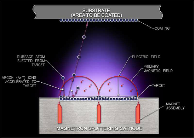
The plasma under high pressure is used to “sputter” metal atoms out of the “target”. These high-energy atoms are deposited on a wafer near the sputtering target material. Higher pressures result in better step coverage due to more random angular delivery. The excess energy of the ions also helps increase surface mobility (the movement of atoms on the surface).
Advantages: Better step coverage, less radiation damage than E-beam evaporation, easier to deposit alloys.
Disadvantages: Some plasma damage including implanted argon. Good for ohmics, not Schottky diodes.
Vacuum Evaporation
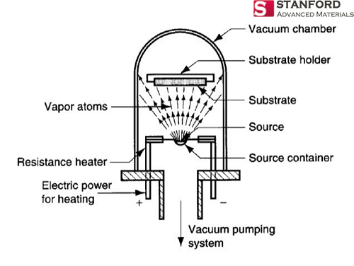
Evaporation is based on the concept that there exists a finite “vapor pressure” above any material. The material either sublimes (direct solid to vapor transition) or evaporates (liquid to vapor transition).
Advantages: Highest purity (Good for Schottky contacts) due to low pressures.
Disadvantages: Poor step coverage, forming alloys can be difficult, lower throughput due to low vacuum.
PVD Film Morphology
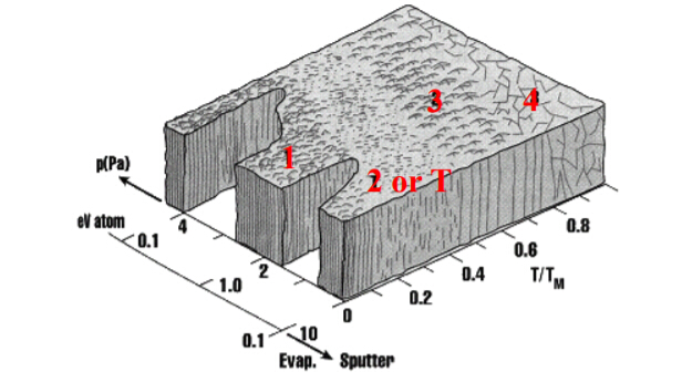
1.) Porous and/or Amorphous —> Results from poor surface mobility =low temperature, low ion energy (low RF power/DC bias or higher pressures=less acceleration between collisions).
2.) “T-zone”: Small grain polycrystalline, dense, smooth and high reflectance (the sweet spot for most metal processes) Results from higher surface mobility =higher temperature or ion energy
3.) Further increases in surface mobility result in columnar grains that have rough surfaces. These rough surfaces lead to poor coverage in later steps.
4.) Still further increases in surface mobility result in large (non-columnar) grains. These grains can be good for diffusion barriers (less grain boundary diffusion due to fewer grains) but pose problems for lithography due to light scatter off of large grains, and tend to be more rigid leading to more failures in electrical lines.
For more information, please visit https://www.sputtertargets.net/.