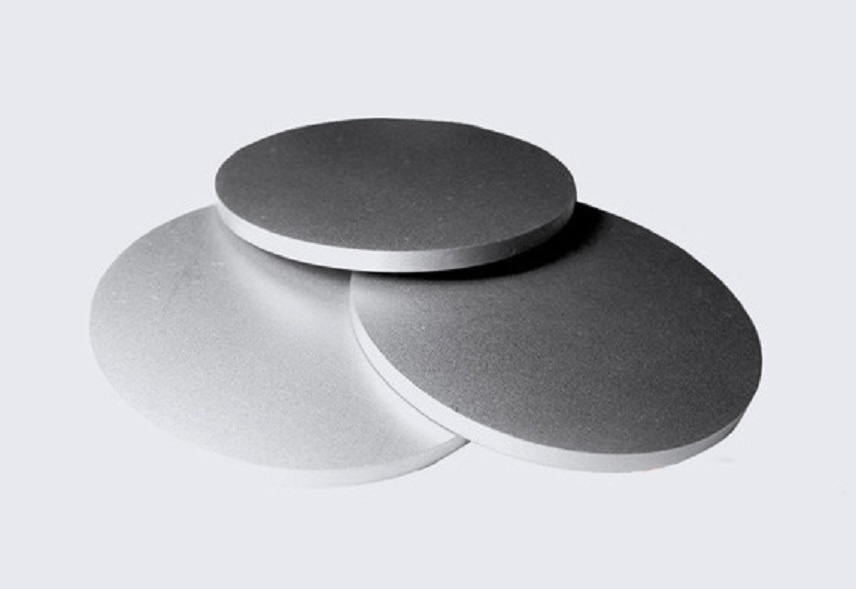
Sputtering targets are materials used to make thin films for many high-tech products, like those in electronics, cars, and renewable energy. Two important types are Indium Tin Oxide (ITO) and iron sputtering targets, which help create coatings that conduct electricity and protect surfaces. As technology changes, new trends are making these materials more efficient, affordable, and better for the environment. Here’s what we can expect in the future.
Making Better Use of Materials
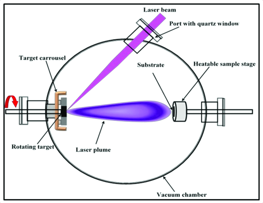
One of the biggest problems in sputtering is the waste of materials. Current sputtering methods often use only a small part of the target, which leads to waste and higher costs.
New Ways to Reduce Waste
To fix this, new methods are being developed to use more of the target material. For example, rotating targets and better magnetron designs can help spread out the use of the material more evenly. This means less waste and lower costs. New power technologies can also make the sputtering process use less energy. These changes can help both ITO and iron sputtering be more efficient and environmentally friendly.
Finding New Materials to Use
ITO is popular for things like touchscreens, displays, and solar panels because it is clear and conducts electricity well. But it depends on indium, which is a rare and expensive metal.
Looking for Other Options
Scientists are looking for other materials that can do the same job as ITO but are easier to find and less expensive. Some good options might be aluminum-doped zinc oxide (AZO) or graphene-based materials. These materials can offer similar benefits without the high cost or supply problems of indium. This shift could lead to new designs and uses for future devices.
Improving How Sputtering Targets Are Made
The quality of sputtering targets affects how well the thin films they create will perform. So, better ways to make these targets are becoming more important.
Better Production Techniques
New methods in powder metallurgy can help create a more uniform material with fewer impurities. Improved bonding methods can make the targets stronger and less likely to have defects. Also, new casting techniques can help produce larger and more consistent targets, leading to fewer mistakes and better-quality films. These improvements are important for products like screens, solar cells, and electronics that need high-performance coatings.
Focusing on Recycling and Sustainability
With growing concerns about the environment, recycling sputtering targets, especially those with rare materials like indium, are becoming more important.
Developing New Recycling Methods
Future trends will likely focus on better recycling techniques to recover valuable materials from used targets. Improved chemical and mechanical methods could make it easier to get back indium and other rare elements. This approach will reduce waste and lower costs, while also supporting a circular economy where materials are reused, reducing the need for new resources.
Using Digital Technology
Digital tools are changing how sputtering is done by using technologies like IoT (Internet of Things), AI (Artificial Intelligence), and machine learning.
Smarter Manufacturing
These tools help control the sputtering process in real time, monitor equipment, and predict when maintenance is needed, preventing breakdowns. For ITO and iron sputtering, this means better production, less downtime, and higher quality. By using data analysis, these technologies can also help find new ways to improve the process, making it more adaptable to changing needs.
Finding New Uses in the Market
As new uses for sputtered films are discovered, demand for ITO and iron sputtering targets is likely to grow in different markets.
Expanding into New Areas
For example, ITO is becoming more popular in flexible electronics and wearable devices that need materials to be both flexible and conductive. At the same time, iron sputtering targets are being used in energy storage technologies, like batteries, to improve performance and lifespan. As these markets expand, so will the need for ITO and iron-sputtering targets, opening up new opportunities.
Conclusion
At Stanford Advanced Materials, we aim to lead in these future trends. With our experience in high-quality sputtering targets, we are ready to meet the changing needs of our customers and support new technology. Check out our range of sputtering targets today to see how we can help you stay ahead in this evolving industry.