The properties of the thin film are determined by the manufacturing method, and different methods have their own advantages and disadvantages. Commonly used preparation processes include magnetron sputtering, chemical vapor deposition, vacuum evaporation, pulsed laser deposition, etc. Among them, magnetron sputtering deposition technology has been widely researched and applied due to its high film formation rate and good uniformity.
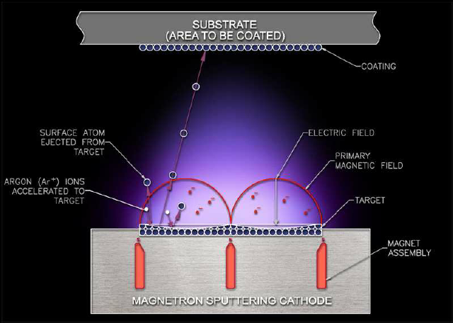
Magnetron Sputtering
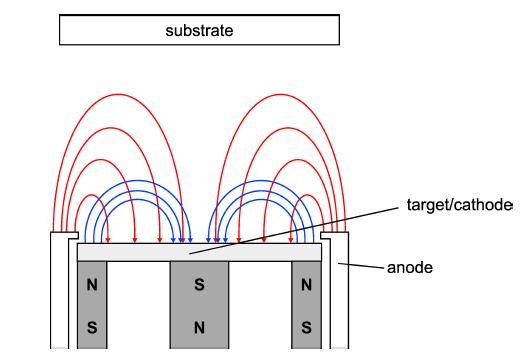
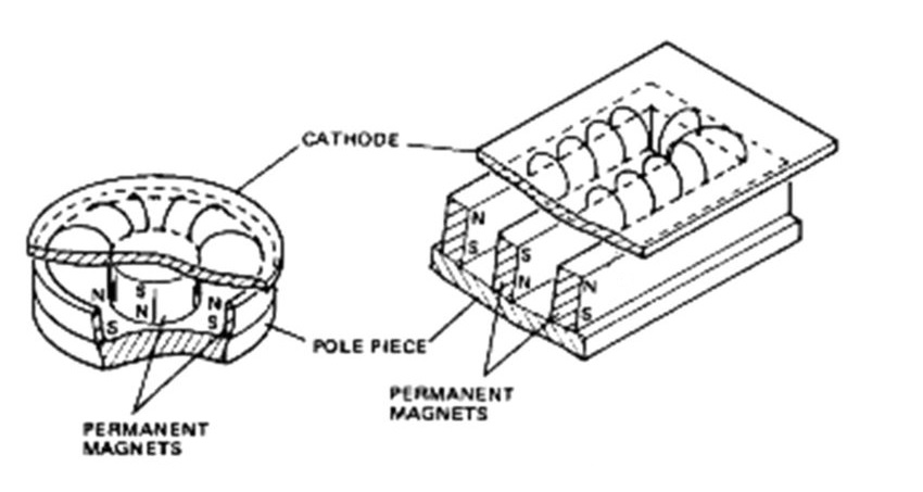
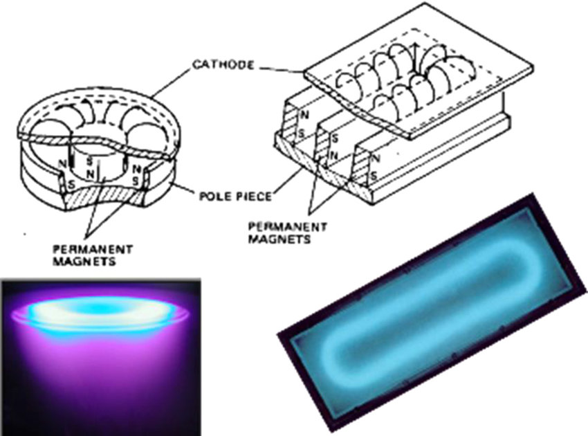
The basic principle of the method is that under the action of electric and magnetic fields, the accelerated high-energy particles (A, +) bombard the surface of the target, and after the energy is exchanged, the atoms on the surface of the target escape from the original lattice, and finally, the sputtering particles are deposited on the surface of the substrate and react with oxygen atoms to form an oxide film. The magnetron sputtering process is characterized by excellent optical and electrical properties of the film deposited at low temperatures. In addition, it has the advantages of a high deposition rate, low substrate temperature, good film adhesion, easy to control, and large-area film formation. Therefore, it has become the most researched and widely used film-forming technology in industrial production today as well as a research hotspot in ITO film preparation technology.
Chemical Vapor Deposition
The chemical vapor deposition method is a process in which a gaseous reactant (including a gaseous reactant that becomes a vaporized condensed matter after evaporation) is chemically reacted on the surface of the substrate to deposit a film. This chemical reaction occurring on the surface of the substrate is usually the thermal decomposition and in-situ oxidation of the source material. The reaction system selected by the CVD method must satisfy:
(1) At the deposition temperature, the reactant must have a sufficiently high vapor pressure;
(2) The chemical reaction product must be in a gaseous state except for the solid matter deposited on the substrate;
(3) The vapor pressure of the deposit should be low enough to ensure good adsorption on a substrate having a certain temperature.
Vacuum Evaporation
The vacuum evaporation method is a method in which a raw material of a to-be-formed film in an evaporation vessel is vaporized from a surface to form a vapor stream, and is incident on a surface of the substrate to react with a gas to form a film in a vacuum chamber. A high-quality ITO film can be prepared by the electron beam evaporation deposition method, in which the evaporation substance is In2O3 doped with SnO2, and the mass percentage of SnO2 is 10%. Under suitable process conditions, the deposited film has a minimum resistivity of 4×10⁻⁴ Ω•cm and an average transmittance in the visible range of more than 90%.
Pulsed Laser Deposition
The pulsed laser deposition (PLD) process is a very competitive new vacuum physical deposition process developed in recent years. Compared with other processes, it has the advantages of precise control of stoichiometry, synthesis, and deposition, and no requirement for the shape and surface quality of the target, so the surface of the solid material can be processed without affecting the material body.
Stanford Advanced Materials(SAM) is a global sputtering targets manufacturer which supplies high-quality and consistent products to meet our customers’ R&D and production needs. Please visit https://www.sputtertargets.net/ for more information.