Metal Molybdenum Target Used in Mobile Phone LCD Screen

Nowadays, mobile phones have become the most indispensable thing for the masses. Mobile phone displays are also becoming more and more high-end, such as full-screen designs, small bang designs, and so on.

One of the most important steps in making a mobile phone LCD screen is thin film coating, using magnetron sputtering to sputter the molybdenum target onto the liquid crystal glass to form a Mo thin film. Molybdenum thin films have the advantages of high melting point, high electrical conductivity, low specific impedance, good corrosion resistance and good environmental performance. Compared with the chromium film, the specific impedance and film stress of the molybdenum film are only half of that.

As an advanced film material preparation technology, sputtering has two characteristics of “high speed” and “low temperature”. It concentrates ions into a high-speed ion stream in a vacuum to bombard a solid surface. The kinetic energy exchange between the ions and the atoms on the solid surface causes the atoms on the solid surface to leave the target and deposit on the surface of the substrate to form a nano (or micro) film. The bombarded solid is a material for depositing a thin film by sputtering, which is called a sputtering target.

mobile phone lcd screen

In the electronics industry, molybdenum sputtering targets are mainly used for flat panel displays, electrodes and wiring materials for thin film solar cells, and barrier materials for semiconductors. These are based on its high melting point, high electrical conductivity, low specific impedance, good corrosion resistance, and good environmental performance.

Molybdenum used in components of LCDs can greatly improve the brightness, contrast, color, and life of the LCD. One of the major applications for molybdenum sputtering targets in the flat panel display industry is in the TFT-LCD field.

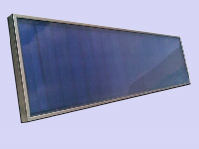
In addition to the flat panel display industry, with the development of the new energy industry, the application of molybdenum sputtering targets on thin film solar photovoltaic cells is also increasing. The molybdenum sputtering target mainly forms a CIGS (Copper Indium Gallium Selenide) thin-film battery electrode layer by sputtering. Among them, molybdenum is at the bottom of the solar cell, and as a back contact of the solar cell. It plays an important role in the nucleation, growth, and morphology of the CIGS thin film crystal.

For more information, please visit https://www.samaterials.com/.

Solar Thin Film and Its Technical Advantages

Thin-film solar cells refer to thin films with thicknesses ranging from a few nanometers to tens of microns attached to the solar surface, which make thin-film cells lighter in weight. Thin-film solar cells are used in building-integrated photovoltaics as translucent photovoltaic glass materials that can be laminated to windows.

As a second-generation solar technology, thin-film technology is more affordable than the traditional first-generation c-Si technology, but is less efficient. Therefore, in recent years, people have also paid more attention to the development of sputtering materials and thin film coating technology, and are committed to improving the efficiency of thin film technology. And now it has improved significantly. Laboratory cell efficiencies for CdTe and CIGS are now over 21%, better than polysilicon, the main material currently used in most solar photovoltaic systems. And the life expectancy of thin-film solar cells is also extended to 20 years or more.

Thin film solar cells are made by depositing one or more thin layers or thin films of photovoltaic materials on a substrate such as glass, plastic or metal. In the deposition process, the coating source material used are usually sputtering targets or evaporation materials. Commonly used thin-film solar cell categories include cadmium telluride (CdTe) thin films, copper indium gallium selenide (CIGS) thin films, and gallium arsenide (GaTe) thin films.

The target materials corresponding to the three thin films mentioned above are important materials for the thin film coating of solar cells. Among them, cadmium telluride targets account for 50% of the solar market. On a life cycle basis, CdTe PV has the smallest carbon footprint, lowest water usage, and shortest energy payback time of all solar technologies. With an energy payback period of less than a year, CdTe can reduce carbon emissions faster without short-term energy shortages.

The CIGS sputtering target is composed of four metal elements, namely copper (Cu), indium (In), gallium (Ga) and selenium (Se), and it is also one of the representatives of commonly used targets in the solar industry. CIGS thin film has the advantages of strong light absorption, good power generation stability and high conversion efficiency, which can enable solar cells to generate electricity for a long time during the day and generate a large amount of electricity. CIGS has great advantages in photovoltaic building-integrated applications. At the same time, with the improvement of CIGS conversion efficiency, the self-sufficiency rate of CIGS as a photovoltaic building power supply built with glass curtain walls is also increasing.

GaAs thin-film solar cells have an efficiency of up to 28.8%, which is considered the highest efficiency of all thin films. Gallium arsenide is also resistant to damage from moisture, radiation and UV light. These properties make GaAs thin films an excellent choice for aerospace applications with increased UV and radiation.

For more information, please visit https://www.sputtertargets.net/.