Introduction
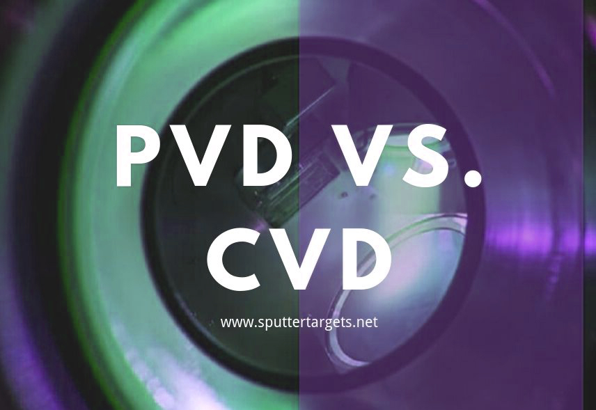
Physical Vapor Deposition (PVD) and Chemical Vapor Deposition (CVD) are essential coating techniques used in various industries. Both methods offer distinct advantages and drawbacks, influencing their suitability for specific applications. This article provides an integrated comparison of PVD and CVD, highlighting their respective strengths and weaknesses.
Understanding PVD and CVD
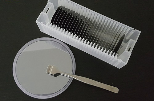
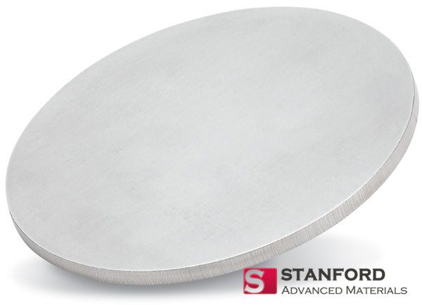
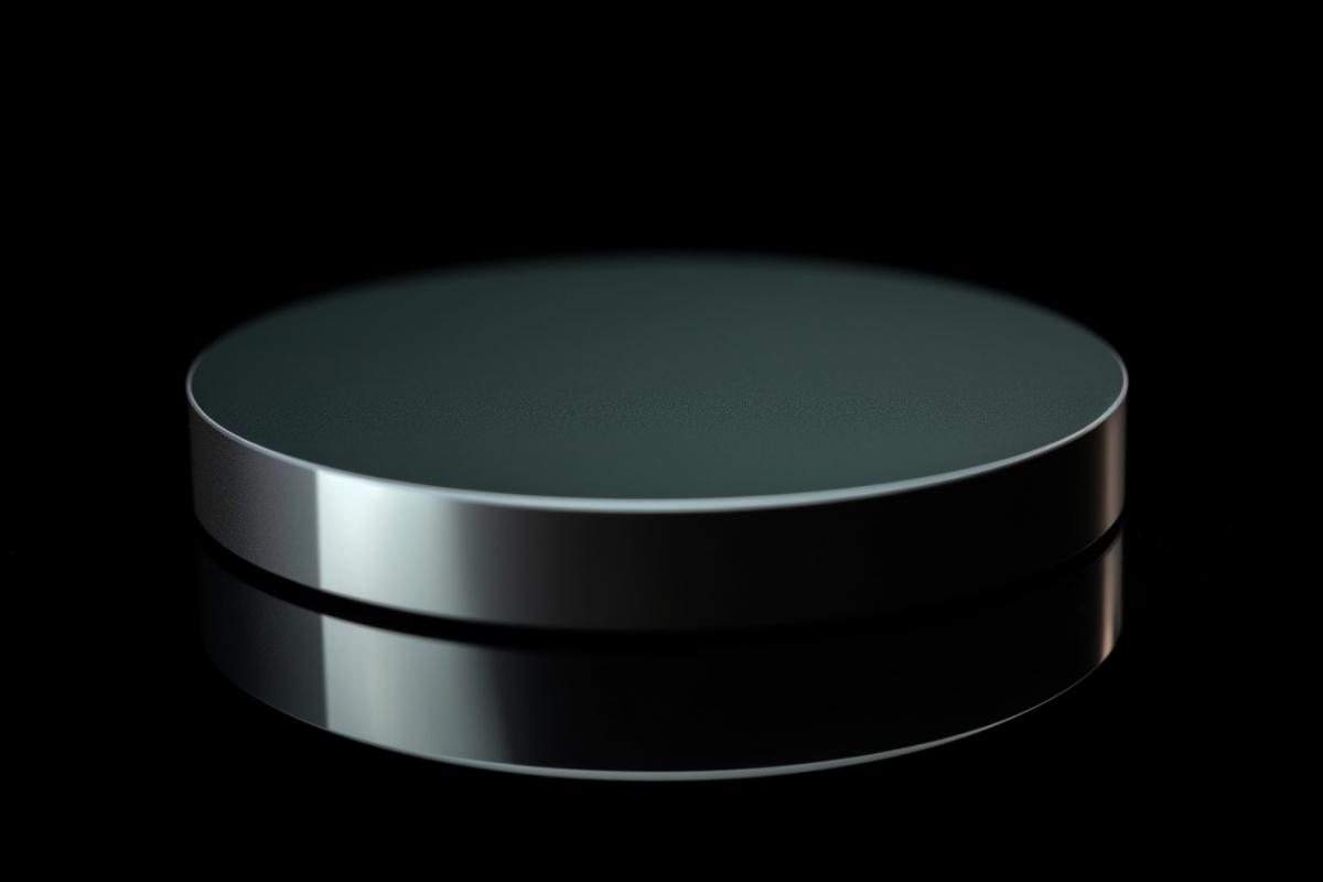
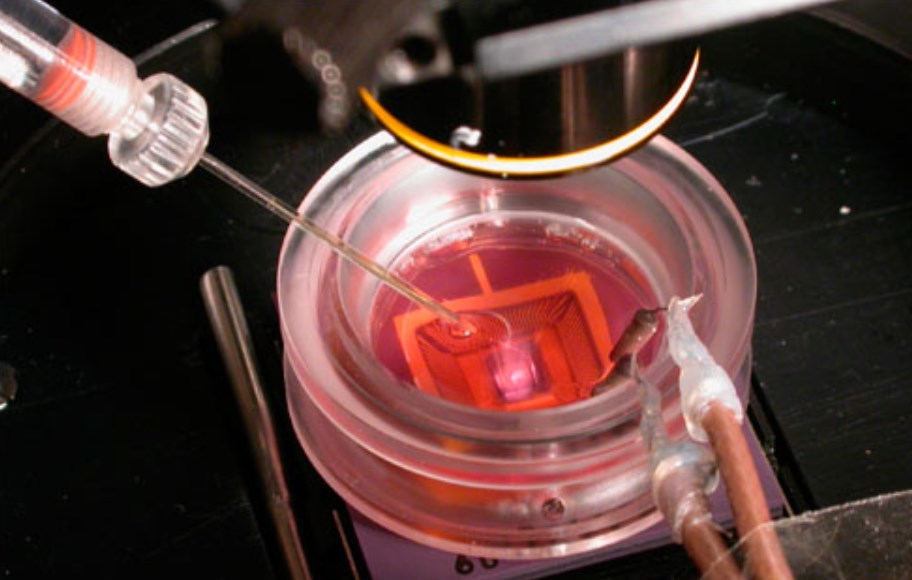
PVD involves the physical transfer of material from a source to a substrate through processes like sputtering or evaporation. Typically operating at lower temperatures, PVD is advantageous for coating heat-sensitive materials. In contrast, CVD relies on chemical reactions to deposit a thin film on the substrate. This process occurs at higher temperatures and involves gaseous precursors that decompose or react to form the coating.
Advantages and Disadvantages of PVD
PVD is well-regarded for its lower temperature requirements, making it ideal for applications involving heat-sensitive substrates. The process is environmentally friendly, producing minimal toxic by-products, and it results in high-purity coatings with excellent adhesion. However, PVD has its limitations. The need for a direct line of sight between the material source and the substrate restricts its effectiveness on complex geometries. Additionally, the deposition rates in PVD are generally slower than those in CVD, which can impact efficiency in large-scale productions. Despite the lower temperatures, certain PVD processes may still negatively affect heat-sensitive substrates, necessitating careful process control.
Advantages and Disadvantages of CVD
CVD excels in providing uniform coatings, even on substrates with intricate shapes. This uniformity makes it advantageous for applications where coating conformity is critical. CVD also offers higher deposition rates, making it efficient for mass production and reducing overall processing time and costs. Furthermore, CVD can deposit a diverse range of materials, including metals, ceramics, and polymers, offering versatility in various industrial applications. However, CVD’s high-temperature requirements can limit its use with temperature-sensitive substrates. The process also produces toxic by-products, necessitating stringent safety protocols and effective waste management systems. Additionally, CVD systems are typically more complex and costly to operate and maintain compared to PVD, which can be a significant drawback for smaller operations.
Applications
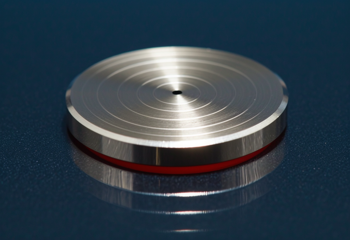
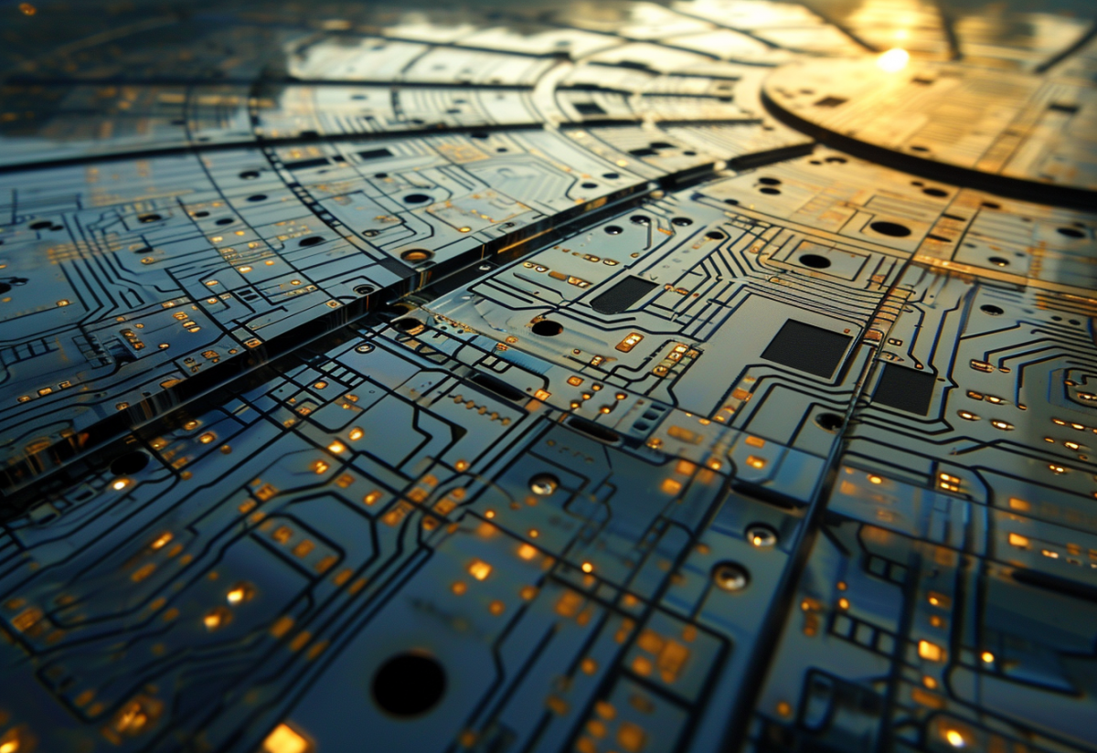
PVD finds extensive use in the electronics industry, creating thin films for semiconductors and other electronic components. It is also employed in decorative coatings, enhancing the appearance and durability of consumer goods like watches and jewelry. In the tooling industry, PVD provides hard coatings for cutting tools, significantly improving their durability and performance by reducing wear and friction.
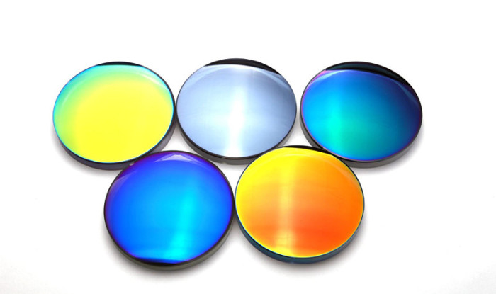
CVD is commonly used in aerospace for protective coatings on turbine blades and other components exposed to high temperatures and harsh environments. In the medical field, CVD enhances the biocompatibility of implants and medical tools, making them safer and more effective for patient use. The optics industry uses CVD to produce anti-reflective and other specialized coatings for optical instruments, improving their performance and longevity.
Conclusion
Deciding between PVD and CVD depends on specific application requirements, including temperature tolerance, coating uniformity, and production scale. PVD is favored for its lower temperature operations, environmental benefits, and high-purity coatings. Conversely, CVD is preferred for its efficiency in providing uniform coatings and material versatility, despite its higher operational complexity and cost. Understanding these nuances is crucial for selecting the optimal coating technique for your industrial applications, ensuring both performance and cost-effectiveness.
For further detailed information, you can read this article PVD vs. CVD: In-depth Comparison.