Introduction:
In the realm of high-temperature applications, graphite crucibles emerge as unsung heroes, playing a crucial role in metallurgy, foundries, and laboratories. This guide is a comprehensive exploration of the proper handling of graphite crucibles, emphasizing their significance, best practices, and ways to extend their lifespan.
Understanding the Significance of Graphite Crucibles:
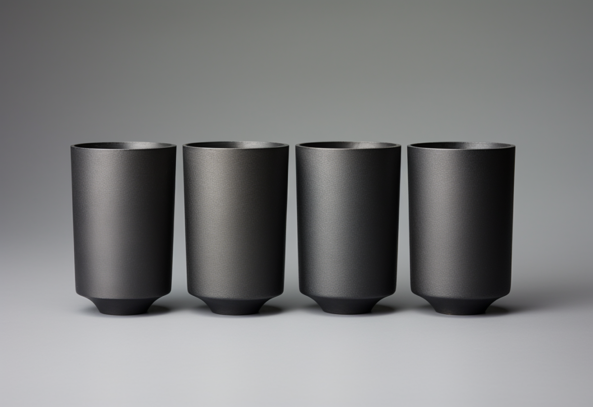
Graphite crucibles, crafted from high-quality graphite materials, are indispensable in processes involving extreme temperatures. Their thermal stability, resistance to chemical corrosion, and durability make them the preferred choice for applications such as metal melting, alloy production, and material analysis in laboratories.
Best Practices for Graphite Crucible Handling:
- Pre-Use Inspection:
Before deploying a graphite crucible, conduct a thorough inspection. Check for any visible cracks, chips, or signs of wear. Identifying potential issues beforehand prevents crucible failure during crucial processes.
- Proper Installation:
Ensure the crucible is properly installed in the furnace or melting apparatus. Improper seating can lead to uneven heating and premature wear, impacting the crucible’s performance.
- Temperature Gradation:
Graphite crucibles excel in extreme temperatures, but a gradual increase in temperature is crucial. Sudden thermal shocks can lead to cracks, compromising the crucible’s integrity. Follow manufacturer guidelines for recommended heating and cooling rates.
- Avoiding Thermal Cycling:
Minimize unnecessary thermal cycling, especially rapid temperature changes, as these can induce stress on the crucible material. Gradual and controlled temperature adjustments preserve the crucible’s structural integrity.
- Optimal Filling Levels:
Overfilling or underfilling a crucible can impact its performance. Adhere to recommended filling levels, ensuring efficient heat transfer and preventing the risk of spillage or damage.
Extending the Lifespan of Graphite Crucibles:
- Regular Cleaning:
After each use, clean the graphite crucible meticulously. Remove residual materials and contaminants to prevent cross-contamination during subsequent uses. This practice contributes to the crucible’s longevity.
- Protective Coatings:
Consider applying protective coatings to the crucible’s interior surface. Coatings like boron nitride can enhance resistance to chemical reactions and minimize metal adhesion, promoting a longer crucible lifespan.
- Storage Conditions:
Proper storage is essential. Keep crucibles in a dry environment to prevent moisture absorption, which can lead to internal cracks during heating.
- Avoiding Impact Damage:
Handle graphite crucibles with care to prevent accidental impacts. Even minor dents or dings can compromise their structural integrity and lead to premature failure.
Troubleshooting Common Issues:
- Cracking:
If a crucible develops cracks, assess their severity. Minor cracks might be manageable with proper coatings, but extensive damage may necessitate replacement.
- Metal Contamination:
Metal contamination can occur due to crucible wear. Regular inspections and cleaning help identify and mitigate this issue.
Conclusion:
Mastering the art of handling graphite crucibles is pivotal in ensuring their longevity and optimal performance in high-temperature applications. From proper installation to meticulous cleaning, each step contributes to the crucible’s resilience. By adhering to these best practices, industries and laboratories can harness the full potential of graphite crucibles, ensuring precision and efficiency in their critical processes.
Further Reading: Graphite Crucibles Used for Metal Smelting