Manufacturing processes have always been evolving, and with the advancements in technology, companies are constantly looking for ways to improve efficiency and reduce costs. One such method that has gained popularity in recent years is the use of chromium pellets for thermal evaporation. These pellets, made of high-purity chromium metal, are used in vacuum deposition processes to create thin films on various substrates. The benefits of using chromium pellets for thermal evaporation are numerous, including improved film quality, reduced manufacturing costs, and increased production rates.
In this article, we will explore the advantages of using chromium pellets in manufacturing and why it has become the preferred method for many industries. So, let’s dive in and discover the world of thermal evaporation and the benefits of using chromium pellets.
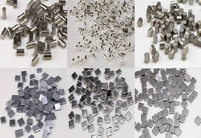
What are Chromium Pellets for Thermal Evaporation?
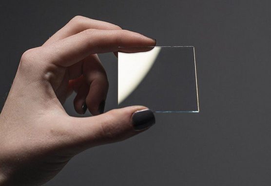
Chromium pellets are small, cylindrical-shaped pieces of high-purity chromium metal that are used in thermal evaporation. Thermal evaporation is a vacuum deposition process, where a material is heated to its evaporation point, and the vaporized material is condensed onto a substrate to form a thin film. Chromium pellets are one of the most popular evaporation materials used in the manufacturing industry, as they offer several advantages over other materials commonly used for thermal evaporation.
Advantages of Using Chromium Pellets
There are several advantages of using chromium pellets for thermal evaporation. The first advantage is improved film quality. Chromium pellets produce high-quality films with excellent adhesion, uniformity, and smoothness. The films produced using chromium pellets are also very stable and have good chemical and mechanical properties, making them ideal for a wide range of applications.
The second advantage of using chromium pellets is reduced manufacturing costs. Chromium pellets have a high evaporation rate, which means that less material is needed to produce the same amount of film. This results in reduced material costs, as well as reduced energy costs, as less energy is required to evaporate the material.
The third advantage is increased production rates. Due to its high evaporation rate, more chromium pellets can be evaporated in a shorter amount of time. This results in increased production rates, which can help companies meet their manufacturing goals faster and more efficiently.
Properties of Chromium Pellets
Chromium pellets are made of high-purity chromium metal, which means that they have excellent physical and chemical properties. Chromium is a hard, lustrous metal that has a high melting point and is resistant to corrosion. Chromium pellets are also very stable and have good mechanical and chemical properties, making them ideal for a wide range of applications.
Comparison of Chromium Pellets with Other Evaporation Materials
Chromium pellets are one of the most popular evaporation materials used in the manufacturing industry, but there are several other materials that are also commonly used. These include aluminum, gold, silver, and copper, among others. While each of these materials has its own advantages and disadvantages, chromium pellets are often preferred due to their excellent film quality, reduced manufacturing costs, and increased production rates.
Applications of Chromium Pellets in Manufacturing
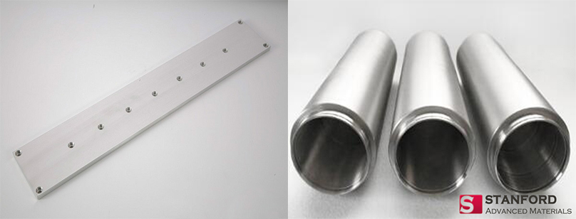
Chromium pellets are used in a wide range of manufacturing applications. Some of the most common applications include the production of thin films for electronics, optics, and solar cells. Chromium pellets are also used in the production of decorative coatings, as well as in the production of hard coatings for cutting tools, molds, and dies.
How to Use Chromium Pellets for Thermal Evaporation
Using chromium pellets for thermal evaporation is a relatively simple process. The first step is to load the pellets into a crucible, which is then placed into the evaporation system. The system is then evacuated to a high vacuum, and the pellets are heated to their evaporation point using an electron beam or resistive heating. The vaporized material is then condensed onto a substrate to form a thin film.
Maintenance and Storage of Chromium Pellets
To ensure the longevity and optimal performance of chromium pellets, proper maintenance, and storage are essential. Chromium pellets should be stored in a dry, cool place, away from moisture and other contaminants. When not in use, the pellets should be stored in an airtight container to prevent oxidation. Before use, the pellets should be cleaned using a mild solvent to remove any surface contaminants.
Where to Buy Chromium Pellets for Thermal Evaporation
Chromium pellets for thermal evaporation can be purchased from a wide range of suppliers. It is important to choose a reputable supplier that offers high-purity chromium pellets that are free from contaminants. One of the most popular suppliers of chromium pellets is Stanford Advanced Material (SAM).
Conclusion
In conclusion, using chromium pellets for thermal evaporation is a highly effective method for producing high-quality films in a wide range of manufacturing applications. The benefits of using chromium pellets include improved film quality, reduced manufacturing costs, and increased production rates. With proper maintenance and storage, chromium pellets can provide optimal performance and longevity, making them an excellent investment for any manufacturing company.