Introduction
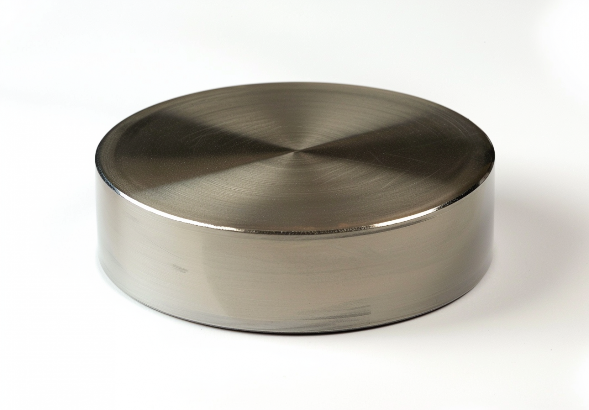
Titanium (Ti) is a widely used material in industries requiring high strength, lightweight properties, and exceptional resistance to extreme temperatures and corrosion. Titanium sputtering targets, commonly used in physical vapor deposition (PVD) processes, play a crucial role in producing thin films for various applications. This article explores the properties, advantages, and applications of titanium sputtering targets, emphasizing their ability to perform under high temperatures. For a comprehensive comparison of materials that excel in similar environments, refer to Top 10 Sputtering Target Materials That Can Withstand High Temperatures.
Key Properties of Titanium Sputtering Targets
Titanium stands out due to its unique combination of physical and chemical properties, making it an excellent choice for high-temperature sputtering applications:
- High Melting Point:
Titanium boasts a melting point of approximately 1668°C (3034°F), allowing it to maintain stability and performance in extreme thermal environments. - Corrosion Resistance:
Titanium forms a protective oxide layer on its surface, which enhances its resistance to oxidation and corrosion in harsh conditions. - Strength and Durability:
Titanium is lightweight yet strong, making it ideal for thin-film deposition processes that demand durability. - Thermal Stability:
The material remains structurally stable during prolonged exposure to high temperatures, ensuring consistent thin-film deposition.
Why High-Temperature Resistance is Important in Sputtering Targets
During sputtering, the target material is bombarded by high-energy ions, causing atoms to eject and deposit as a thin film on a substrate. This process generates significant heat, making thermal resistance critical. Titanium sputtering targets meet this challenge by:
- Maintaining Structural Integrity:
Titanium’s stability prevents warping or deformation under intense heat, ensuring a steady sputtering process. - Ensuring Film Quality:
The material’s high-temperature resistance supports uniform atom ejection, resulting in high-quality thin films with consistent properties. - Extending Target Lifespan:
Titanium’s durability and thermal performance reduce the frequency of target replacements, saving time and cost in industrial applications.
Applications of Titanium Sputtering Targets
Titanium sputtering targets are used in various industries for their ability to produce robust, high-performance thin films. Some key applications include:
- Semiconductors:
Titanium is commonly used in the semiconductor industry for barrier layers, interconnects, and other thin-film applications. Its resistance to heat and oxidation ensures reliability in electronic devices. - Optical Coatings:
Titanium sputtering targets are used to produce anti-reflective coatings, decorative films, and protective layers for optical lenses, mirrors, and displays. - Aerospace and Automotive:
Titanium’s lightweight and high-strength properties make it a preferred material for coating components in aerospace and automotive industries, where high temperatures and stress are common. - Medical Devices:
Titanium is biocompatible, making it ideal for creating thin films used in medical implants, surgical tools, and diagnostic equipment. - Decorative Coatings:
Titanium sputtering targets are also used to create wear-resistant and visually appealing coatings for consumer goods such as watches, jewelry, and electronic devices.
Advantages of Titanium Sputtering Targets
Titanium sputtering targets offer several benefits for industries requiring high-performance materials:
- High Temperature Performance:
Titanium maintains its integrity and efficiency under extreme heat, ensuring reliability in demanding applications. - Corrosion Resistance:
Its natural oxide layer protects it from environmental degradation, enhancing the durability of thin films. - Lightweight Strength:
Titanium combines lightness with strength, making it easier to handle while providing robust performance. - Versatility:
Suitable for a wide range of applications, titanium sputtering targets are a preferred choice across industries.
Choosing the Right Titanium Sputtering Target
When selecting a titanium sputtering target, consider the following factors:
- Purity:
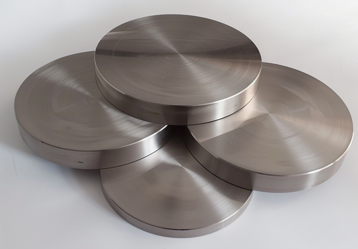
High-purity titanium targets are essential for applications requiring minimal impurities, such as semiconductor and medical industries. - Target Size and Shape:
Ensure the dimensions and form of the target match your sputtering system requirements. Customized sizes are often available. - System Compatibility:
Verify that the sputtering system’s power and parameters align with the titanium target’s properties for optimal performance.
Conclusion
Titanium sputtering targets are indispensable for industries that require materials capable of withstanding high temperatures, corrosion, and physical stress. Whether used in semiconductors, optics, aerospace, or medical applications, titanium ensures the production of high-quality thin films with superior durability and performance.
Stanford Advanced Materials (SAM) provides high-quality titanium sputtering targets designed to meet the diverse needs of various industries. With a commitment to precision and reliability, SAM ensures that your thin-film deposition processes achieve exceptional results. For more information on high-temperature sputtering materials, explore Top 10 Sputtering Target Materials That Can Withstand High Temperatures.
Read more: Everything You Need to Know About Titanium Sputtering Target