Indium Tin Oxide (ITO) is a vital material in the world of modern displays, particularly in Liquid Crystal Displays (LCDs). Found in televisions, computer monitors, smartphones, and a myriad of other electronic devices, ITO serves as a transparent electrode, a role that is central to creating clear, bright, and energy-efficient screens. Understanding how ITO works and why it is essential in LCDs can provide insight into the technology behind our daily displays.
The Function of ITO in LCD Technology
At the core of every LCD is a layer of liquid crystals, sandwiched between two glass substrates. These liquid crystals do not produce light by themselves; instead, they manipulate external light to form images. This is where Indium Tin Oxide (ITO) comes in.
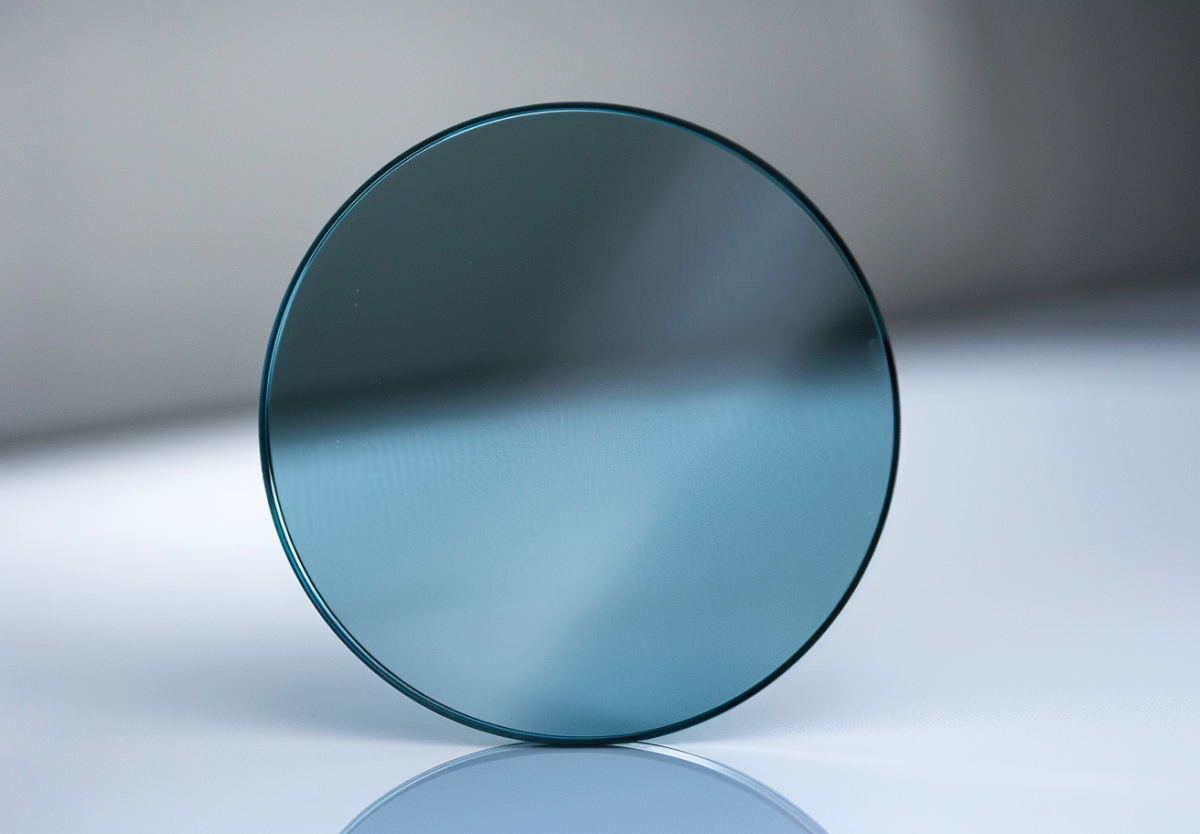
ITO is a compound that combines indium oxide and tin oxide, forming a material that is both conductive and transparent. When applied as a thin film to one or both glass substrates in an LCD, it acts as an electrode that conducts electricity while allowing light to pass through. This dual property is what makes ITO so valuable in display technology.
An electric current passing through the ITO layer generates an electric field that affects the orientation of the liquid crystals. Depending on their orientation, the liquid crystals either block or allow light to pass through. By carefully controlling the voltage applied across the ITO electrodes, manufacturers can adjust the liquid crystals’ alignment, creating varying shades, colors, and levels of brightness that form the images you see on your screen.
Benefits of Using ITO in LCDs
- High Transparency and Clarity: The primary advantage of ITO in LCDs is its high level of transparency. This property ensures that maximum light reaches the viewer without being absorbed or reflected by the conductive layer. As a result, LCDs using ITO provide a bright, clear display that is easy to read even in well-lit environments. The glare reduction further enhances visibility and readability, making screens more comfortable for prolonged use.
- Improved Contrast and Color Accuracy: By controlling the orientation of the liquid crystals precisely, ITO allows for a high contrast ratio, where the difference between the darkest blacks and the brightest whites is maximized. This precise control also enhances color accuracy, making colors more vibrant and true to life. The ability to finely adjust the electric field helps create smooth gradients and sharp images, improving the overall visual experience.
- Energy Efficiency: ITO contributes significantly to the energy efficiency of LCDs. Because it allows for precise control over the liquid crystals with minimal electrical input, LCDs require less power to operate. This is particularly important in battery-powered devices such as laptops, tablets, and smartphones, where energy consumption directly impacts battery life. The energy savings provided by ITO make these devices more sustainable by reducing their energy footprint.
- Durability and Reliability: In addition to its optical and electrical properties, ITO is also highly durable and resistant to environmental factors such as moisture and temperature fluctuations. This resilience ensures that displays maintain their performance and longevity, even under challenging conditions. For manufacturers, this means fewer defects and returns, and for consumers, it translates to a longer-lasting display with consistent performance over time.
Applications Beyond LCDs
While ITO is best known for its use in LCDs, its applications extend to other types of displays and devices as well. ITO is commonly used in organic light-emitting diode (OLED) displays, touch screens, and photovoltaic cells, where its transparent and conductive properties are equally advantageous. As display technology continues to evolve, ITO remains a critical material for achieving the best performance, efficiency, and reliability.
Read more: How Indium Tin Oxide (ITO) Improves Flat-Panel Displays
Conclusion
Indium Tin Oxide is an essential material in the production of modern LCDs, offering benefits that range from high transparency and clarity to improved energy efficiency and durability. Its unique combination of properties makes it invaluable in creating bright, vivid, and efficient displays. As the technology landscape continues to shift, ITO’s contributions will remain at the forefront of display innovation, enabling clearer, more energy-efficient screens in the devices we rely on every day.
Get more info on SAM’s website.