Advantages and Disadvantages of Pulsed Laser Deposition (PLD)

Introduction to Pulsed Laser Deposition (PLD)

In the world of materials science, the quest for precision and versatility in thin film preparation has led to the development of several advanced techniques, among which Pulsed Laser Deposition (PLD) stands out.

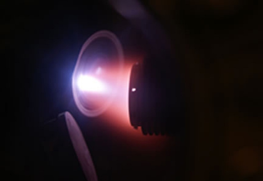
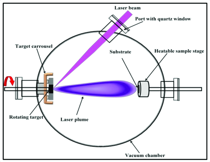
PLD, also known as Pulsed Laser Ablation, harnesses the power of a laser to bombard the surface of a target material. This process elevates the surface temperature significantly, producing high-temperature and high-pressure plasma (T > 104K). The material then deposits on various substrates to form a thin film. This technique is celebrated for its ability to create films with unparalleled precision, catering to a wide range of applications from microelectronics to optical technologies.

Simplified schematic diagram illustrating the pulsed laser deposition (PLD) set-up.
Simplified schematic diagram illustrating the pulsed laser deposition (PLD) set-up. Ogugua, Simon & Swart, H. & Ntwaeaborwa, Odireleng. (2020). Latest Development on Pulsed Laser Deposited ThinFilms for Advanced Luminescence Applications. Coatings. 10. 1078. 10.3390/coatings10111078.

Advantages of PLD

Multi-component Films

One of the hallmark advantages of PLD is its adeptness at producing multi-component films that maintain the desired stoichiometric ratios with ease. This characteristic is particularly beneficial in applications requiring precise chemical compositions, making PLD a preferred method for developing advanced functional materials.

High Deposition Rate and Flexibility

PLD boasts a high deposition rate, ensuring a swift test period and minimal substrate temperature requirements. This efficiency, coupled with the uniformity of the films prepared, positions PLD as a highly effective method for thin film deposition. Moreover, the process’s inherent simplicity and flexibility signal its vast development potential and compatibility across a broad spectrum of materials science endeavors.

Adjustable Process Parameters

The ability to arbitrarily adjust process parameters is another feather in PLD’s cap. This flexibility allows for the easy preparation of multilayer films and heterojunctions, with no limitation on the type of PLD targets. The adaptability in choosing multi-target components further underscores PLD’s versatility in meeting diverse material preparation needs.

Non-polluting and Easy Control

Utilizing UV pulsed lasers as the energy source for plasma generation, PLD stands out as a non-polluting technique. This aspect, combined with the method’s ease of control, ensures that PLD aligns with the growing demand for environmentally friendly and easily manageable manufacturing processes in the production of thin film materials.

Disadvantages of PLD

Despite its numerous advantages, PLD is not without its challenges. One notable issue is the presence of molten small particles or target fragments in the deposited film, which can significantly compromise the quality of the film. These particles, sputtered during the laser-induced explosion, introduce defects that detract from the film’s integrity.

The feasibility of PLD for large-area deposition also remains unproven, limiting its application in industries requiring expansive film coverage. Coupled with an average deposition rate that is slow relative to other methods, these limitations suggest areas where PLD may benefit from further refinement and innovation.

Moreover, considering the cost and scale of laser film preparation equipment, PLD’s current applicability appears confined to high-tech fields such as microelectronics, sensor technology, optical technology, and new material films. This niche positioning highlights the need for continued development to expand PLD’s utility across a broader range of applications.

Stanford Advanced Materials (SAM) and PLD

In the landscape of thin film preparation, the role of reliable materials suppliers cannot be overstated. Stanford Advanced Materials (SAM) Corporation emerges as a global leader in providing a diverse array of sputtering targets, including metals, alloys, oxides, and ceramic materials. These materials are pivotal for PLD and other thin film deposition techniques, underscoring SAM’s contribution to advancing the frontiers of materials science and engineering.

Conclusion

Pulsed Laser Deposition (PLD) presents a compelling technique in the preparation of thin films, offering a unique blend of precision, versatility, and environmental friendliness. While its advantages pave the way for innovative applications, the method’s limitations highlight areas ripe for research and development. As the field continues to evolve, partnerships with materials suppliers like Stanford Advanced Materials (SAM) will be crucial in harnessing PLD’s full potential, driving forward the technological advancements that rely on high-quality thin films.

Thinning and Coating Process of Mobile Phone Cover Glass

According to the needs of various terminal applications, glass cover panels require various optical glass processing processes such as cutting, edging, drilling, polishing, thinning, chemical strengthening, printing, laser engraving and coating. Today we will introduce the thinning and coating of mobile phone cover glass, which are the most important parts of the whole manufacturing process.

Cover glass thinning process

The glass mentioned in this article is not the 3mm, 5mm, 8mm or even 10mm glass for civil use, but the cover glass for electronic products such as smartphones and tablet computers. Among the glasses currently on the market, the thinnest is 0.15 mm. There is a special thinning process that reduces the thickness of the glass.

Since Steve Jobs started using Corning Gorilla Glass for his iPhones, there emerges a new component for electronic products—cover glass. At the same time, the pursuit of thinner and lighter in the industry is also urging glass manufacturers to make changes to make thinner cover glass.

iPhone cover glass
iPhone cover glass

Currently, the thinnest glass of gorilla can be made 0.4mm, and the Asahi Glass can make 0.2mm glass. In general, people’s expectations for cover glass are nothing more than two:

1. Reduce the space occupied by the glass.

2. Make the glass cover a certain flexibility.

Mobile phone cover glass thinning process

There are not many processes for glass cover thinning: pre-cleaning—etching and thinning—–secondary cleaning——-grinding (single or double sided)—–post-cleaning—–check the package

Pre-cleaning: Remove the stain on the surface of the glass cover. It is one of the key steps affecting the effect of thinning.

Etching and thinning:  using acid and alkali to etch the glass cover achieve the purpose of thinning. The conditions and parameters (time, potash ratio, temperature, etc.) vary from manufacturer to manufacturer, which is the technical secret of the manufacturer.

Secondary cleaning: Clean the residue of the glass cover.

Grinding: To obtain a bright, flat surface. It is one of the key processes for appearance assurance and thickness tolerance control.

Post-cleaning: Clean the remaining grinding powder.

Check the packaging: The standard for the appearance of the glass is different depending on the requirements of the customer.

Mobile phone cover glass thinning treatment

1, multiple pieces of upright soak

2, waterfall flow processing

3, single piece vertical spray

Cover glass coating process

At present, vacuum magnetron sputtering coating technology is a widely used thin film deposition technology. The continuous development of sputtering technology and the exploration of new functional films have enabled the application of magnetron sputtering coating technology to be extended to many productions and scientific research fields.

magnetron sputtering system
magnetron-sputtering-system

magnetron sputtering coating applications

In the field of microelectronics, as a non-thermal coating technology, magnetron sputtering coating technology is mainly applied to materials that are not suitable for chemical vapor deposition or metal organic chemical vapor deposition. Moreover, using magnetron sputtering can obtain a large-area uniform film.

Magnetron sputtering technology is also used in optical films such as antireflection glass, low emissivity glass and transparent conductive glass. In the production of transparent conductive glass, the ITO conductive glass prepared by sputtering has an average transmittance of 90% or more in the visible light range.

In the modern machining industry, the use of magnetron sputtering technology to produce surface functional films, super hard films and self-lubricating films can effectively improve surface hardness, composite toughness, wear resistance and high temperature resistance and chemical stability, thus improve the service life of coated products.

In addition, magnetron sputtering coating technology also plays an important role in the research of high temperature superconducting thin films, ferroelectric thin films, giant magnetoresistive thin films, thin film luminescent materials, solar cells, and memory alloy thin films.

Magnetron sputtering coating advantages

Magnetron sputtering coating technology has become one of the main technologies of the industrial coating due to its remarkable advantages:

(1) Simple operation and easy control. In the coating process, if the sputtering conditions such as working pressure and electric power are relatively stable, the deposition rate is relatively stable.

(2) The deposition rate is high. When depositing most of the metal, especially the high melting point metal and oxide, such as tungsten, aluminum TiO2 and ZrO2 film, it has a high deposition rate.

(3) Low temperature of the substrate. Compared to two-pole sputtering or thermal evaporation, magnetron sputtering reduces the heating of the substrate, which is quite advantageous for achieving the sputter coating of the fabric.

(4) The sputtered film is strong. The sputtered film has excellent adhesion to the substrate and its mechanical strength is also improved.

(5) The sputtered film is dense and uniform. From the photomicrograph, the surface morphology of the sputtered film is fine and uniform.

(6)The sputtered films all have excellent properties. For example, sputtered metal films generally achieve good optical properties, electrical properties, and certain special properties.

(7) Easy to mass produce. The magnetron source can be expanded as required, so large-area coatings are achievable. In addition, sputtering can work continuously, and the coating process is easy to control automatically, so that the industrial assembly line can be realized.

(8) Environmentally friendly. Conventional wet plating produces waste liquid, waste residue, and exhaust gas, causing serious pollution to the environment. The magnetron sputtering coating method has high production efficiency while does not cause environmental pollution.

Please visit https://www.sputtertargets.net/ for more information.

Copper Sulfide Sputtering Targets Are The Best Sputtering Materials

Sputtering is a thin film deposition process in the modern technology world of CDs, semiconductors, disk drives and optical devices industries. Sputtering is the process at an atomic level, where the atoms are automatically sputtered out from the sputtering materials and then be deposited on another substrate, such as a solar panel, semiconductor wafer or optical device. It is an effect of the severe bombard of the high energy particles on the target.

In general, sputtering occurs only when kinetic energy is said to be bombarding particles at very high speeds, which is much higher than a normal thermal energy. At the atomic level, this makes thin film deposition more precise and accurate than that by melting the source material using conventional thermal energy.

Copper Sulfide is the best material for Sputtering Targets. It can be molded into the shape of Plates, Discs, Step Targets, Column Targets and Custom-made. Copper Sulfide is a combination of two materials—Copper and Sulphur. The chemical name of the product is CuS, which offers you the Copper Sulfide product with more than 99 percent purity.


Copper
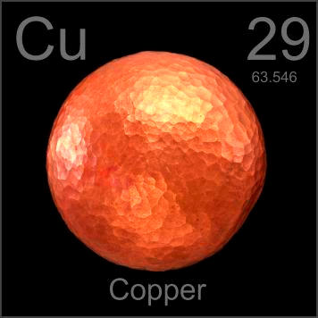
Cyprus is the original source material for the chemical element Copper. The people of Middle East initially discovered it in 9000 BC. “Cu” is the canonical chemical symbol of copper.


Sulfur
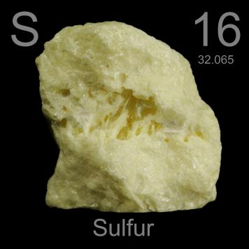
Whereas Sulfur, otherwise known as sulphur, is first introduced in 2000 BC and discovered by Chinese and Indians. It is a chemical name originated from the Sanskrit word ‘sulvere’, and the Latin ‘sulfurium’. Both names are for sulfur.


Copper Sulfide metal discs and plates are highly adhesive and resistant against oxidation and corrosion. Using Copper Sulfide sputtering targets to deposit thin films will not produce highly reflective and extremely conductive films, but can also extensively increase the efficiency of the source energy.

So to achieve the desired noticeable result in a sputtering deposition, the built-up process used to fabricate the Sputtering Targets should be critical. A Copper Sulfide targeted material will give the best result. However, material like only an element, alloys, mixture of elements, or perhaps a compound can be used for the purposes.

For more information about sputtering targets, please visit http://www.sputtertargets.net/.