What is Extreme High Speed Laser Material Deposition(EHLA)?

The German research institute Fraunhofer Institute for Laser Technology has developed a groundbreaking metal part coating process called Extreme High Speed Laser Material Deposition (EHLA). This innovative technique promises to revolutionize the way metal coatings are applied, offering significant improvements in efficiency, speed, and environmental impact.

How EHLA Works

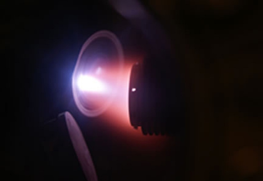
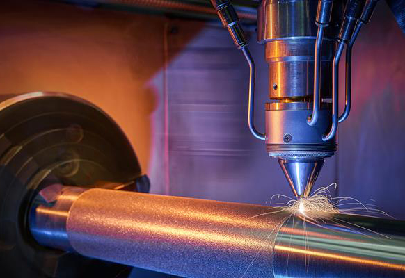
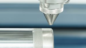
EHLA involves using a laser to create a molten pool on the surface of a component. A precise amount of metal powder is then added to this pool. Unlike traditional laser deposition processes, the powder in EHLA melts completely before it is deposited on the part’s surface. This ensures a thin, uniform coating that is both durable and resource-efficient. Remarkably, EHLA introduces approximately 90% of the material into the desired area, compared to just 50% in other methods.

Extreme High Speed Laser Material Deposition

Speed and Efficiency

The standout feature of EHLA is its exceptional speed. Coating processes using EHLA can be performed at speeds 100 to 250 times faster than conventional laser material deposition techniques. This rapid application rate drastically reduces processing time, making EHLA an attractive option for high-volume production environments.

Heat Sensitivity and Versatility

One of the key advantages of EHLA is its minimal heat generation during processing. This makes it ideal for coating heat-sensitive components without causing thermal damage. Additionally, EHLA is capable of tandem coating processing, which allows for the application of multiple layers or different materials in a single operation. This versatility opens up new possibilities for advanced coatings that can enhance the performance and longevity of metal parts.

Environmental Benefits

EHLA stands out for its environmental friendliness. The process eliminates the need for chromium, a chemical commonly used in traditional coating processes that is harmful to the environment. EHLA uses no hazardous chemicals, making it a safer and more sustainable option. Moreover, the coating adheres to the substrate in a material-locking manner, preventing peeling and ensuring a long-lasting bond.

Applications and Future Prospects

Researchers are excited about the potential applications of EHLA. The process is effective in protecting metal parts from corrosion and wear, extending the life cycle of products. It is compatible with various coatings, including iron, nickel, and cobalt-based alloys, making it suitable for a wide range of industrial applications.

With its impressive speed, efficiency, and environmental benefits, EHLA presents a promising future for metal coating technologies. It offers a sustainable solution that not only enhances the performance of metal parts but also reduces resource consumption and environmental impact.

About Stanford Advanced Materials

Stanford Advanced Materials (SAM) Corporation is a global supplier of various sputtering targets such as metals, alloys, oxides, and ceramic materials. If you are interested in learning more about EHLA or our range of products, please visit our website at SAM Sputter Targets for more information.

Advantages and Disadvantages of Pulsed Laser Deposition (PLD)

Introduction to Pulsed Laser Deposition (PLD)

In the world of materials science, the quest for precision and versatility in thin film preparation has led to the development of several advanced techniques, among which Pulsed Laser Deposition (PLD) stands out.

PLD, also known as Pulsed Laser Ablation, harnesses the power of a laser to bombard the surface of a target material. This process elevates the surface temperature significantly, producing high-temperature and high-pressure plasma (T > 104K). The material then deposits on various substrates to form a thin film. This technique is celebrated for its ability to create films with unparalleled precision, catering to a wide range of applications from microelectronics to optical technologies.

Simplified schematic diagram illustrating the pulsed laser deposition (PLD) set-up.
Simplified schematic diagram illustrating the pulsed laser deposition (PLD) set-up. Ogugua, Simon & Swart, H. & Ntwaeaborwa, Odireleng. (2020). Latest Development on Pulsed Laser Deposited ThinFilms for Advanced Luminescence Applications. Coatings. 10. 1078. 10.3390/coatings10111078.

Advantages of PLD

Multi-component Films

One of the hallmark advantages of PLD is its adeptness at producing multi-component films that maintain the desired stoichiometric ratios with ease. This characteristic is particularly beneficial in applications requiring precise chemical compositions, making PLD a preferred method for developing advanced functional materials.

High Deposition Rate and Flexibility

PLD boasts a high deposition rate, ensuring a swift test period and minimal substrate temperature requirements. This efficiency, coupled with the uniformity of the films prepared, positions PLD as a highly effective method for thin film deposition. Moreover, the process’s inherent simplicity and flexibility signal its vast development potential and compatibility across a broad spectrum of materials science endeavors.

Adjustable Process Parameters

The ability to arbitrarily adjust process parameters is another feather in PLD’s cap. This flexibility allows for the easy preparation of multilayer films and heterojunctions, with no limitation on the type of PLD targets. The adaptability in choosing multi-target components further underscores PLD’s versatility in meeting diverse material preparation needs.

Non-polluting and Easy Control

Utilizing UV pulsed lasers as the energy source for plasma generation, PLD stands out as a non-polluting technique. This aspect, combined with the method’s ease of control, ensures that PLD aligns with the growing demand for environmentally friendly and easily manageable manufacturing processes in the production of thin film materials.

Disadvantages of PLD

Despite its numerous advantages, PLD is not without its challenges. One notable issue is the presence of molten small particles or target fragments in the deposited film, which can significantly compromise the quality of the film. These particles, sputtered during the laser-induced explosion, introduce defects that detract from the film’s integrity.

The feasibility of PLD for large-area deposition also remains unproven, limiting its application in industries requiring expansive film coverage. Coupled with an average deposition rate that is slow relative to other methods, these limitations suggest areas where PLD may benefit from further refinement and innovation.

Moreover, considering the cost and scale of laser film preparation equipment, PLD’s current applicability appears confined to high-tech fields such as microelectronics, sensor technology, optical technology, and new material films. This niche positioning highlights the need for continued development to expand PLD’s utility across a broader range of applications.

Stanford Advanced Materials (SAM) and PLD

In the landscape of thin film preparation, the role of reliable materials suppliers cannot be overstated. Stanford Advanced Materials (SAM) Corporation emerges as a global leader in providing a diverse array of sputtering targets, including metals, alloys, oxides, and ceramic materials. These materials are pivotal for PLD and other thin film deposition techniques, underscoring SAM’s contribution to advancing the frontiers of materials science and engineering.

Conclusion

Pulsed Laser Deposition (PLD) presents a compelling technique in the preparation of thin films, offering a unique blend of precision, versatility, and environmental friendliness. While its advantages pave the way for innovative applications, the method’s limitations highlight areas ripe for research and development. As the field continues to evolve, partnerships with materials suppliers like Stanford Advanced Materials (SAM) will be crucial in harnessing PLD’s full potential, driving forward the technological advancements that rely on high-quality thin films.

Physical Vapor Deposition: Sputter Coating & Evaporation

Physical vapor deposition processes use vacuum technology to create a sub-atmospheric pressure environment and an atomic or molecular condensable vapor source (from a solid or liquid surface) to deposit thin films and coatings. Sputtering deposition and vacuum evaporation are among the more well known.

physical vapor deposition sputtering evaporation

Sputtering deposition

The sputtering deposition is an etching process that alters the physical properties of a surface. In this process, a gas plasma discharge is set up between two electrodes: a cathode plating material (the sputter coater targets) and an anode material (the substrate). The film made by sputter coating are thin, ranging from 0.00005 – 0.01 mm. Chromium, titanium, aluminum, copper, molybdenum, tungsten, gold, and silver are typical sputter coating targets.

Sputter coated films are used routinely in decorative applications such as watchbands, eyeglasses, and jewelry. Also, the electronics industry relies on heavily sputtered coatings and films, such as thin film wiring on chips and recording heads as well as magnetic and magneto-optic recording media. Companies also use sputter deposition to produce reflective films for large pieces of architectural glass used in the automotive industry. Compared to other deposition processes, sputter deposition is relatively inexpensive.

vacuum coating

Vacuum Evaporation

The vacuum evaporation is a process of reducing the wastewater volume through a method that consists of concentrating a solution by eliminating the solvent by boiling. In this case, it is performed at a pressure lower than atmospheric pressure. Thus, the boiling temperature is much lower than that at atmospheric pressure, thereby resulting in notable energy savings. The basic components of this process consist of: evaporation pellets,  heat-exchanger, vacuum, vapor separator, and condenser.

Vacuum evaporation is used in the semiconductor, microelectronics, and optical industries and in this context is a process of depositing thin films of material onto surfaces. High-purity films can be obtained from a source evaporation material with high purity. The source of the material that is going to be vaporized onto the substrate can be a solid in any shape or form (usually pellets). The versatility of this method trumps other deposition processes. Also, when the deposition is not desired, masks are utilized to define the areas on the substrate for control purposes.

Information from Stanford Advanced Materials. Please visit https://www.sputtertargets.net/ for more information.

Introduction to Physical Vapor Deposition Technologies

Thin Film Deposition

Thin film deposition technology refers to the preparation of thin films on the surface of materials used in the fields of machinery, electronics, semiconductors, optics, aviation, transportation and etc., in order to impart certain properties (such as heat resistance, wear resistance, corrosion resistance, decoration, etc.) to these materials.

The two most common forms of thin film deposition techniques are physical vapor deposition (PVD) and chemical vapor deposition (PVD).

Physical Vapor Deposition —PVD

PVD is a process that achieves the transformation of the atoms from the source materials to the substrate to deposit a film by physical mechanisms such as thermal evaporation or sputtering.

PVD includes evaporation, sputtering and ion plating.

Evaporation

Evaporation is a common method of thin-film deposition. It is also called vacuum evaporation because the source material is evaporated in a vacuum. The vacuum allows the vapored particles to travel directly to the substrate, where they condense and deposit to form a thin film.

Evaporation (PVD)
Evaporation (PVD)

Sputtering

Sputtering is a physical vapor deposition (PVD) method of thin film deposition. It is a process whereby particles are ejected from a solid target material (sputtering target) due to the bombardment of the target by energetic particles.

Sputtering (PVD)
Sputtering (PVD)

Ion Plating

Ion plating is a physical vapor deposition (PVD) process which uses a concurrent or periodic bombardment of the substrate, and deposits film by atomic-sized energetic particles.

Ion Plating (PVD)
Ion Plating (PVD)

Characteristics of the main physical vapor deposition method

Among the above three methods, although Ion plating’s film adhesion and density are better, due to technical limitations, the other two methods (evaporation and sputtering) are currently more widely used. In general, sputtering is the best PVD technology.

Stanford Advanced Materials (SAM) is one of the most specialized sputtering targets manufacturers, please visit https://www.sputtertargets.net/ for more information.