Role of Advanced Coating Technologies in Industry 4.0

Introduction

Standing on the cusp of the Fourth Industrial Revolution, commonly known as Industry 4.0, we find ourselves amid a transformative period in manufacturing. This article delves into the integral role of advanced coating technologies, connecting their evolution to the emerging trends in PVD technology. From the intricacies of smart manufacturing to the precision of engineering, we explore how Industry 4.0 propels the demand for innovative surface coatings.

Understanding Industry 4.0

Industry 4.0 signifies a monumental shift in manufacturing, embodying the integration of digital technologies into every facet of industry. This revolution harnesses the power of artificial intelligence, the Internet of Things (IoT), machine learning, data analytics, and advanced robotics. It builds upon the digital foundations laid by its predecessors, promising a connected, intelligent, and data-driven industrial landscape.

The Intersection of Industry 4.0 and PVD Technology

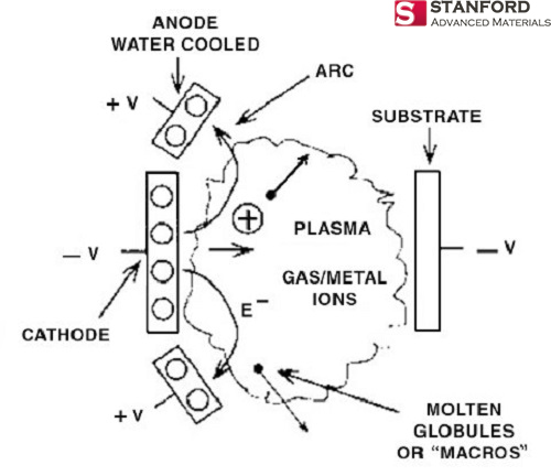
At its core, Industry 4.0 seamlessly merges technologies like artificial intelligence, the Internet of Things, and data analytics. This integration profoundly influences surface engineering, with Physical Vapor Deposition (PVD) technology playing a pivotal role. In the context of Industry 4.0, PVD processes transcend conventional surface coating; they become integral components within a connected, intelligent manufacturing ecosystem. This ecosystem relies on real-time adaptability and data-driven insights, with PVD coatings facilitating these features.

Precision Coatings for Smart Manufacturing

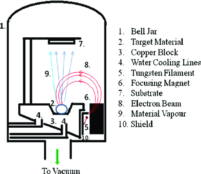
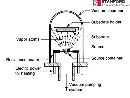
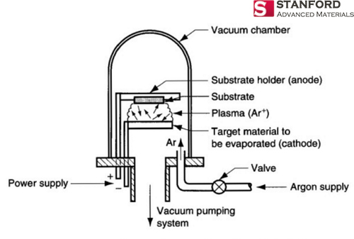
In the realm of Industry 4.0, precision is paramount. Advanced coating technologies, particularly those facilitated by PVD processes, contribute significantly to the precision required for smart manufacturing. Coatings engineered at the nanoscale are crucial for components demanding precision, such as sensors, actuators, and microelectromechanical systems (MEMS). These coatings enhance wear resistance, reduce friction, and provide thermal stability, ensuring the optimal performance of interconnected components within the Industry 4.0 framework.

Real-world Applications

Let’s transition from theory to practice by examining real-world applications where advanced coatings play a pivotal role in smart manufacturing. In aerospace, high-performance coatings withstand extreme conditions and enhance fuel efficiency. In electronics, nanoscale coatings enable device miniaturization and improve overall performance. The automotive industry benefits from PVD coatings providing durability and aesthetics to components. Each application exemplifies the symbiosis between Industry 4.0 principles and advanced PVD coating technologies.

Future Prospects

As we conclude, let’s peer into the prospects of advanced coating technologies within the Industry 4.0 framework. The evolving landscape envisions even more interconnected, intelligent manufacturing systems. PVD technology, with its ability to deliver precisely, tailored coatings, is poised to be a linchpin in this future industrial ecosystem. This integration promises to revolutionize surface engineering, ushering in a new era of precision, efficiency, and unprecedented possibilities.

Conclusion

In the era of Industry 4.0, the story of advanced coating technologies and PVD is one of collaboration and innovation. As we navigate the future, the integration of these technologies promises to revolutionize the way we approach surface engineering, setting the stage for a new era of precision, efficiency, and unprecedented possibilities.

Electron Beam Deposition for Film Coating

Introduction

Electron beam deposition is a form of physical vapor deposition (PVD) in which the target anode material is bombarded with a stream of electrons generated by a tungsten filament. Electron beam thin film deposition techniques are widely used in R&D as well as in mass production applications.

Electron beam deposition is performed in a vacuum, typically starting the process at levels below 10-5 Torr. Once a suitable vacuum is reached, a tungsten filament in the electron beam source emits a stream of electrons. This electron beam can be generated in various ways, including thermionic emission, field electron emission, or ion arc source, depending on the design of the source and associated power supply.

In all cases, the negatively charged electrons are attracted to the positively charged anode material. The generated electron beam is accelerated to high kinetic energy and directed towards the material to be deposited on the substrate. This energy is converted into heat by interacting with the atoms of the evaporated material.

The purpose of generating a stream of electrons in an electron beam source is to heat the deposited material to a temperature above a vapor pressure threshold at a given background pressure. The vapor stream is then condensed onto the surface of the substrate.

Schematic representation of electron beam evaporation system depicting various parts.
Schematic representation of electron beam evaporation system depicting various parts.. Mohanty, P. & Kabiraj, Debdulal & Mandal, R.K. & Kulriya, Pawan Kumar & Sinha, Ask & Rath, Chandana. (2014). Evidence of room temperature ferromagnetism in argon/oxygen annealed TiO2 thin films deposited by electron beam evaporation technique. Journal of Magnetism and Magnetic Materials. 355. 240–245. 10.1016/j.jmmm.2013.12.025.

Deposition Rate

As with all thermal evaporation systems, the electron beam deposition rate depends on the temperature of the material being deposited and the vapor pressure (physical constant) of that material. For elemental materials, there is a fixed vapor pressure for any particular background pressure (vacuum) and material temperature. However, for alloys or composites, there may be different partial pressures associated with each component.

Compared with Sputter Coating

Unlike sputter deposition, where individual atoms arrive at the substrate surface with very high velocity and momentum, the thermally generated vapor stream arrives at the substrate surface at a considerably lower velocity, but a much greater velocity. In other words, e-beam deposition rates can be orders of magnitude greater than sputter deposition rates, making e-beam coatings very beneficial for high volume production or thick film requirements. One disadvantage, however, is that the material tends to condense directly on the substrate surface due to the different kinetic energy of the arriving species during electron beam evaporation than that of the sputtered species. In contrast, atoms of sputtered materials tend to penetrate several atomic layers (or more) to the substrate surface before losing momentum and then establishing cohesive bonds in nucleation structures and film growth. Thus sputtered films tend to provide better adhesion properties than thermally evaporated materials.

For more information, please visit https://www.sputtertargets.net/.

Evaporation Coating Experiment: Principle, Purpose & Results

Introduction

In recent years, the rapid economic development and the continuous improvement of people’s living standards have led to the continuous emergence of high-tech thin-film products, especially in the field of electronic materials and components. Vacuum coating technology has also gained significant application in this field.

At present, the common film-forming methods include vapor-phase film-forming method, oxidation method, ion implantation method, diffusion method, electroplating method, coating method, liquid-phase growth method, etc. The vapor generation method can be further subdivided into physical vapor deposition, chemical vapor deposition, and discharge polymerization.

Principle

The experiments listed in this article are related to physical vapor deposition coatings. This method is basically carried out under vacuum, so it is called vacuum coating technology.

Vacuum evaporation, sputter coating, and ion plating are commonly referred to as basic physical vapor deposition thin film preparation techniques. The vacuum evaporation coating method is a method in which the evaporation material of a film to be formed in a vaporization chamber is heated in a vacuum chamber, and atoms or molecules are vaporized from the surface to form a vapor stream, which is incident on the surface of the substrate and condensed to form a solid film.

Evaporation Coating

Purposes

  1. To familiarize yourself with the operating procedures and methods obtained by vacuum;
  2. In order to understand the principle and method of evaporation coating;
  3. To learn how to use evaporation coating technology.

Results

(1) Vacuum conditions during evaporation

When the average free path of the vapor molecules in the vacuum vessel is greater than the distance between the evaporation source and the substrate (called the steaming distance), sufficient vacuum conditions are obtained. For this reason, it is necessary to increase the mean free path of the residual gas to reduce the collision probability of the vapor molecules with the residual gas molecules, and to evacuate the vacuum chamber to a high vacuum.

(2) How to choose evaporation source selection

1 It should have good thermal stability, chemical inactivity; the vapor pressure of the heater itself is sufficient to reach the evaporation temperature.

2 Its melting point should be higher than the evaporation temperature of the evaporated material. The heater should have a large enough heat capacity.

3 The mutual melting of the evaporated material and the evaporation source material must be very low, and it is difficult to form an alloy.

4 The material used for the coil-shaped evaporation source is required to have a good wetting with the evaporation material and a large surface tension.

5 For a case where it is difficult to form a filament, or when the surface tension of the evaporation material and the filament evaporation source is small, a boat-shaped evaporation source can be used.

(3) Main physical processes of thermal evaporation coating

1 Using various forms of thermal energy conversion to vaporize or sublimate the coating material into gaseous particles (atoms, molecules or atomic groups) with certain energy (0.1~0.3eV);

2 Gaseous particles are transported to the substrate by a substantially collision-free linear motion;

3 Particles are deposited on the surface of the substrate and agglomerated into a film.

(4) Factors affecting the quality and thickness of vacuum coating

There are many factors affecting the quality and thickness of the vacuum coating, including the degree of vacuum, the shape of the evaporation source, the position of the substrate, and the temperature of the evaporation source. The solid matter has very low evaporation at normal temperature and normal pressure. The higher the degree of vacuum, the easier it is for the molecules of the evaporation source material to scatter away from the surface of the material. The fewer molecules in the vacuum chamber, the lower the probability that the evaporating molecules will collide with the gas molecules, so that the surface of the substrate can be reached unobstructed straight.

For more information, please visit https://www.samaterials.com/.

How to make the phone case of gradient color like Huawei P20?

Gradient color is popular in 2018

It’s overwhelming how many smartphone models are currently available on the market today.  However, as for the color of the phone, what get are the same old black, white, silver and gray, in glossy or matte.

Well, recently an exciting new trend has emerged. The Huawei P20 series let people see the optimal color design and professional photography. A few months ago, Huawei launched the P20 in Twilight, and the dual-tone gradient inspired by the Aurora Borealis made people feel excited.

Huawei P20
Huawei P20

Before that, HTC also introduced the two-tone gradient scheme. Although it does not offer the popular Twilight color scheme, it does bring us a few appealing options with its latest flagship device.

HTC U11
HTC U11

Samsung has also jumped on board the gradient crazy. The Korean tech giant has unveiled a new version of its Galaxy A9 Star in China which features a sleek purple gradient.

Galaxy A9 Star2
Galaxy A9 Star2

Well, these are just a few examples to show that gradient color is the fashion of the year 2018. Are you curious about how to achieve this kind of gradient color? Is it difficult?

Film coating-Physical vapor deposition

Actually, all the color of the shell is about film coating. A cellphone is made from a variety of metals, with the most common being aluminum alloys, lightweight materials commonly found in the phone case. And the film coating is to apply a colored film on the phone case.

Physical vapor deposition is the most widely used film coating technology. Under vacuum conditions, the surface of the material (usually referred to as the sputtering targets or evaporating pellets) is vaporized into gaseous atoms by physical methods, and is then deposited on the surface of the substrate to form a thin film. The main methods of physical vapor deposition include vacuum evaporation, sputtering coating, plasma coating, ion plating, and molecular beam epitaxy.

How to coat the gradient color

PVD can coat gold, brass, rose gold, silver white, black, smoky, copper, brown, purple, blue, burgundy, bronze and other colors on stainless steel, copper, zinc alloy and other metals. There are many choices and the price is affordable, compared to pure gold or other pure metals. (PVD Coating Materials.pdf) You can refer to our previous article for more information: Introduction to PVD Coatings.

By controlling the parameters of different targets and thickness of the deposited film, the film exhibits different colors (the gradation colors mentioned above) under the reflection, refraction and interference of light. Specifically, in the plating furnace space, bombard a specific sputtering target with ultra-high speed electrons; use a certain mask to cover a part of the ion cloud so that only the other part of the ion cloud can be attached to the substrate and forms a very thin layer of nano-plating; control the thickness of the coating to form a nanometer thickness difference; then spray the background color.

For more information, please visit https://www.sputtertargets.net/.

Introduction to Physical Vapor Deposition Technologies

Thin Film Deposition

Thin film deposition technology refers to the preparation of thin films on the surface of materials used in the fields of machinery, electronics, semiconductors, optics, aviation, transportation and etc., in order to impart certain properties (such as heat resistance, wear resistance, corrosion resistance, decoration, etc.) to these materials.

The two most common forms of thin film deposition techniques are physical vapor deposition (PVD) and chemical vapor deposition (PVD).

Physical Vapor Deposition —PVD

PVD is a process that achieves the transformation of the atoms from the source materials to the substrate to deposit a film by physical mechanisms such as thermal evaporation or sputtering.

PVD includes evaporation, sputtering and ion plating.

Evaporation

Evaporation is a common method of thin-film deposition. It is also called vacuum evaporation because the source material is evaporated in a vacuum. The vacuum allows the vapored particles to travel directly to the substrate, where they condense and deposit to form a thin film.

Evaporation (PVD)
Evaporation (PVD)

Sputtering

Sputtering is a physical vapor deposition (PVD) method of thin film deposition. It is a process whereby particles are ejected from a solid target material (sputtering target) due to the bombardment of the target by energetic particles.

Sputtering (PVD)
Sputtering (PVD)

Ion Plating

Ion plating is a physical vapor deposition (PVD) process which uses a concurrent or periodic bombardment of the substrate, and deposits film by atomic-sized energetic particles.

Ion Plating (PVD)
Ion Plating (PVD)

Characteristics of the main physical vapor deposition method

Among the above three methods, although Ion plating’s film adhesion and density are better, due to technical limitations, the other two methods (evaporation and sputtering) are currently more widely used. In general, sputtering is the best PVD technology.

Stanford Advanced Materials (SAM) is one of the most specialized sputtering targets manufacturers, please visit https://www.sputtertargets.net/ for more information.

PVD vs. CVD: What’s the difference?

PVD vs. CVD: What’s the difference?

In recent years, physical vapor deposition (PVD) and chemical vapor deposition (PVD) have wide applications in various industries to increase the hardness of tools and molds or apply beautiful colors to the products. Thus these two methods are considered as the most attractive surface coating technologies. Then, using the example of cutting tools, let’s make a detailed comparison between these two methods.

Definition

Physical vapor deposition (PVD) uses low-voltage, high-current arc discharge technology under vacuum conditions to evaporate the target and ionize the vaporized material and the gas, and finally make the evaporated material and its reaction deposited on the workpiece.

Continue reading “PVD vs. CVD: What’s the difference?”