

Thin Film Deposition
Thin film deposition technology refers to the preparation of thin films on the surface of materials used in the fields of machinery, electronics, semiconductors, optics, aviation, transportation and etc., in order to impart certain properties (such as heat resistance, wear resistance, corrosion resistance, decoration, etc.) to these materials.
The two most common forms of thin film deposition techniques are physical vapor deposition (PVD) and chemical vapor deposition (PVD).
Physical Vapor Deposition —PVD
PVD is a process that achieves the transformation of the atoms from the source materials to the substrate to deposit a film by physical mechanisms such as thermal evaporation or sputtering.
PVD includes evaporation, sputtering and ion plating.
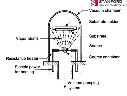
Evaporation
Evaporation is a common method of thin-film deposition. It is also called vacuum evaporation because the source material is evaporated in a vacuum. The vacuum allows the vapored particles to travel directly to the substrate, where they condense and deposit to form a thin film.
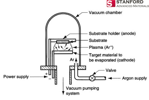
Sputtering
Sputtering is a physical vapor deposition (PVD) method of thin film deposition. It is a process whereby particles are ejected from a solid target material (sputtering target) due to the bombardment of the target by energetic particles.
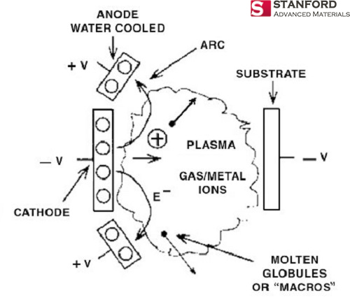
Ion Plating
Ion plating is a physical vapor deposition (PVD) process which uses a concurrent or periodic bombardment of the substrate, and deposits film by atomic-sized energetic particles.
Characteristics of the main physical vapor deposition method
Among the above three methods, although Ion plating’s film adhesion and density are better, due to technical limitations, the other two methods (evaporation and sputtering) are currently more widely used. In general, sputtering is the best PVD technology.
Stanford Advanced Materials (SAM) is one of the most specialized sputtering targets manufacturers, please visit https://www.sputtertargets.net/ for more information.
2 thoughts on “Introduction to Physical Vapor Deposition Technologies”