Introduction
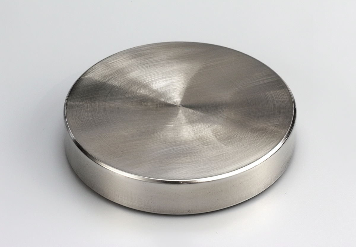
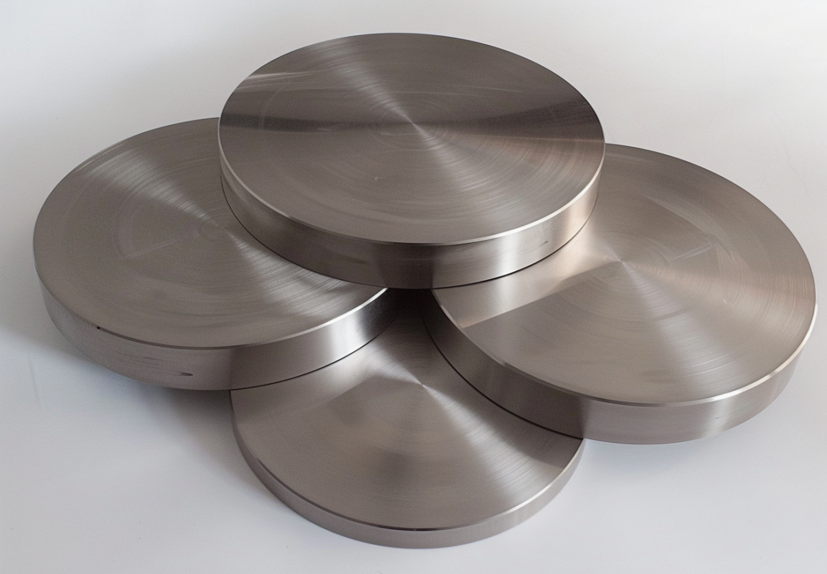
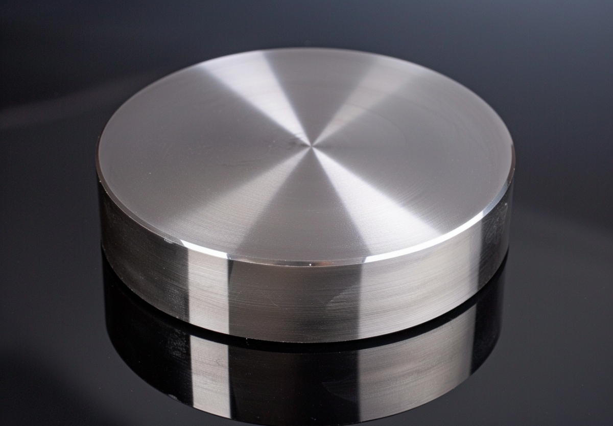
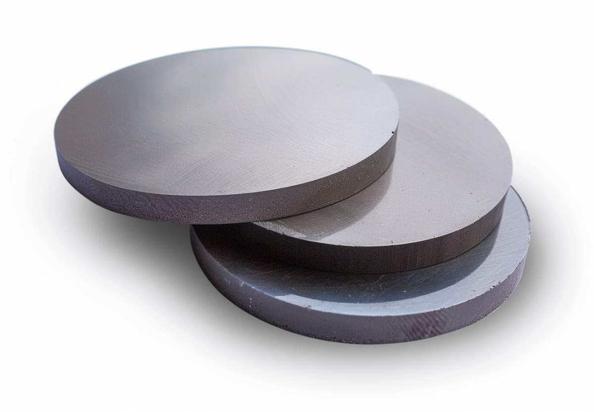
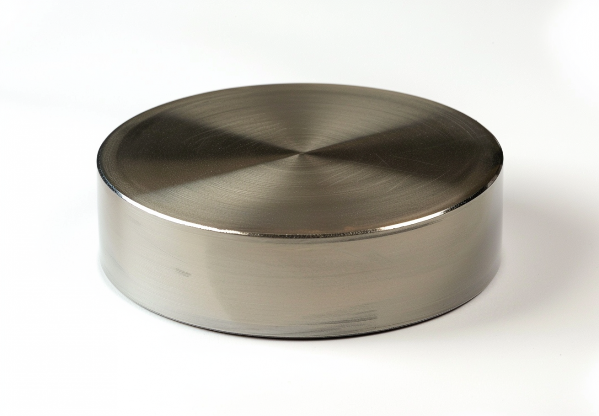
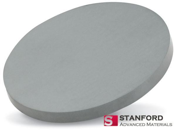
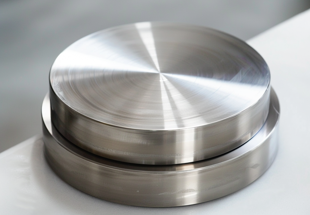
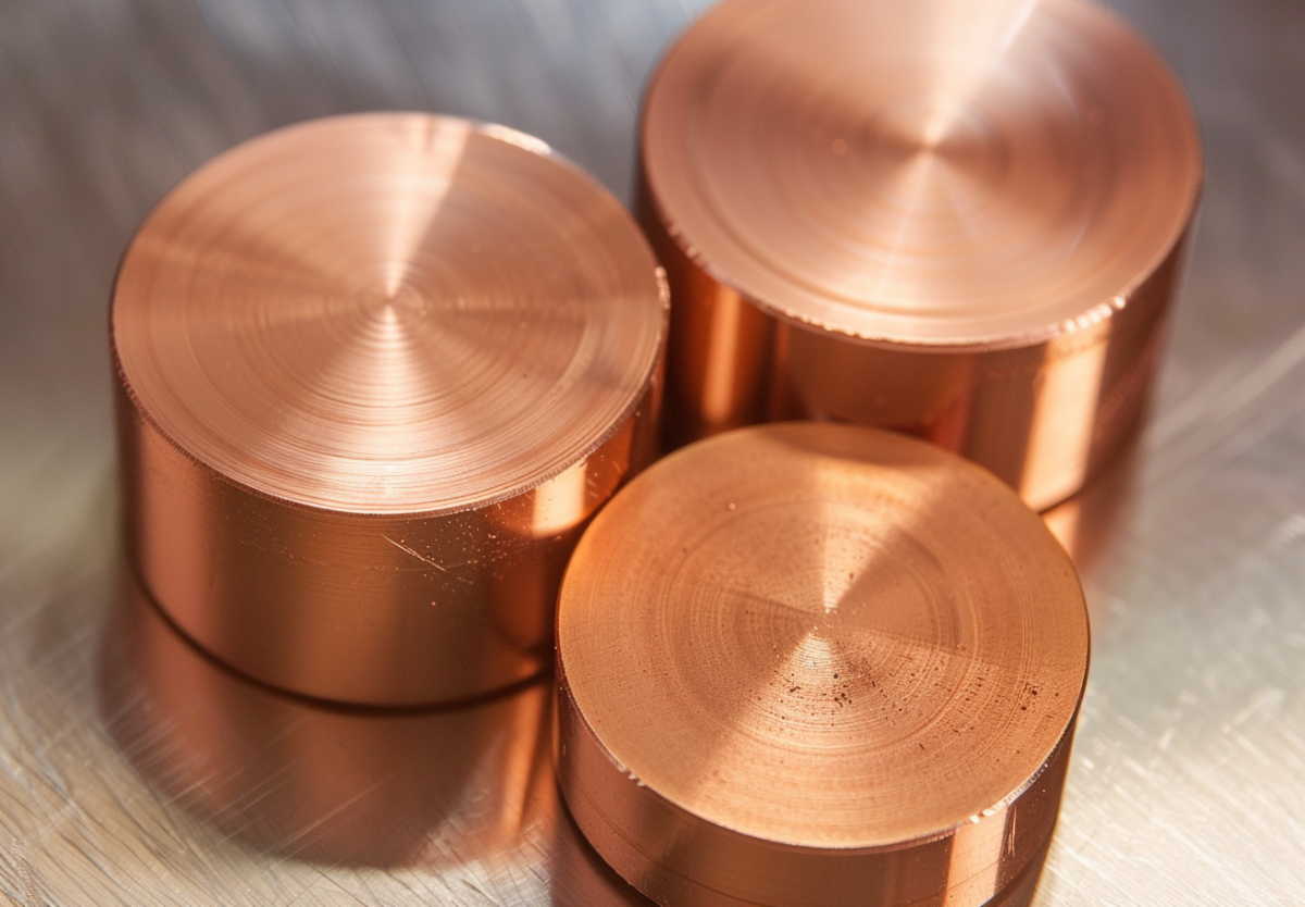
Copper (Cu) is one of the most widely used materials in thin film deposition processes due to its excellent electrical conductivity, thermal properties, and versatility. Copper sputtering targets, in particular, are essential in producing high-performance thin films for a variety of applications, including semiconductor devices, optical coatings, and electrical components. Although copper is highly regarded for its excellent conductivity, its ability to withstand high temperatures during the sputtering process is a critical factor in its selection as a target material. In this article, we will explore the properties of copper sputtering targets, their ability to endure high temperatures, and the benefits they provide in high-temperature sputtering applications.
For a broader view of materials capable of withstanding high temperatures, you can also check out the article Top 10 Sputtering Target Materials That Can Withstand High Temperatures.
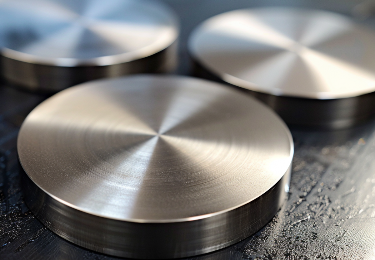
Key Properties of Copper Sputtering Targets
Copper sputtering targets possess several key characteristics that make them suitable for thin film deposition, even in high-temperature environments:
- High Electrical Conductivity: Copper is one of the best conductors of electricity, which is why it is commonly used in applications requiring efficient electrical performance, such as microelectronics and photovoltaics.
- Thermal Conductivity: Copper has excellent thermal conductivity, which helps in efficiently distributing heat during the sputtering process, thus preventing local overheating that could degrade the target or affect the deposition quality.
- Ductility and Malleability: Copper is a relatively soft and ductile metal, allowing it to be shaped and formed into sputtering targets with fine precision. Its malleability also allows the target to absorb some degree of thermal stress without cracking.
- Moderate Melting Point: While copper’s melting point is lower than that of other metals like tungsten or molybdenum (about 1,984°F / 1,085°C), it still has a sufficiently high thermal tolerance for many sputtering applications that do not require extreme heat conditions.
- Corrosion Resistance: Copper is naturally resistant to corrosion in many environments, though it can tarnish and oxidize when exposed to air. During sputtering, the oxidation of copper can sometimes affect film quality, which is why careful control of process parameters is necessary.
Why High-Temperature Resistance Matters for Copper Sputtering Targets
The sputtering process involves bombarding a target with high-energy ions, causing atoms from the target to be ejected and deposited onto a substrate. The temperature generated during this process can cause degradation in some materials, but copper sputtering targets are designed to endure these conditions. High-temperature resistance is crucial for several reasons:
- Maintaining Target Stability: Copper sputtering targets need to withstand the thermal stress generated by the sputtering process without melting, deforming, or breaking apart. If a target fails under heat stress, it can lead to inconsistent deposition and poor film quality.
- Ensuring Consistent Film Quality: As copper is bombarded by ions, it needs to remain stable and provide a consistent release of atoms for uniform film deposition. High-temperature resistance ensures that the copper target does not degrade, which could otherwise lead to uneven films with unwanted impurities.
- Longevity of Sputtering Targets: Copper’s ability to perform well at elevated temperatures increases the operational lifespan of the sputtering target. This is important in industries with high-throughput production where reducing the frequency of target replacements is critical for minimizing downtime and costs.
Applications of Copper Sputtering Targets
Copper sputtering targets are widely used in industries that require the deposition of thin films with superior electrical and thermal conductivity. Key applications include:
- Semiconductor Manufacturing:
Copper is used extensively in the production of integrated circuits (ICs) and microelectronic devices. Copper thin films are often deposited as interconnects due to their high conductivity, making them essential in semiconductor fabrication. - Photovoltaic Cells:
Copper sputtering targets are also employed in the manufacturing of thin-film solar cells, where their excellent conductivity helps in creating efficient solar energy conversion layers. - Magnetic Coatings:
Copper is used in magnetic thin film applications, particularly in data storage devices such as hard drives, where its conductivity and resistance to corrosion are critical for the performance of the device. - Optical Coatings:
Copper thin films are used in optical coatings for mirrors and other optical devices that require high reflectivity and durability. - Electrical Components:
Copper sputtering targets are used in the production of electrical components such as connectors, contacts, and conductors, where their high thermal and electrical conductivity is essential.
Conclusion
Copper sputtering targets are an excellent choice for many applications that require both high conductivity and resistance to moderate to high temperatures. While their melting point is not as high as some other materials like tungsten or molybdenum, copper’s thermal and electrical properties, along with its ductility, make it ideal for many thin-film deposition processes. As mentioned in the article Top 10 Sputtering Target Materials That Can Withstand High Temperatures, copper is among the key materials that offer reliable performance in a wide range of sputtering applications.
Choosing the right material for sputtering targets is crucial for ensuring the quality and longevity of thin films. Copper provides an optimal balance of conductivity, thermal stability, and cost-effectiveness, making it a top choice for industries that demand high-performance thin films.