
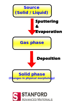
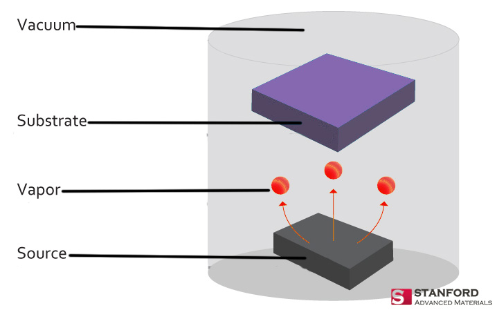
Physical vapor deposition processes use vacuum technology to create a sub-atmospheric pressure environment and an atomic or molecular condensable vapor source (from a solid or liquid surface) to deposit thin films and coatings. Sputtering deposition and vacuum evaporation are among the more well known.
Sputtering deposition
The sputtering deposition is an etching process that alters the physical properties of a surface. In this process, a gas plasma discharge is set up between two electrodes: a cathode plating material (the sputter coater targets) and an anode material (the substrate). The film made by sputter coating are thin, ranging from 0.00005 – 0.01 mm. Chromium, titanium, aluminum, copper, molybdenum, tungsten, gold, and silver are typical sputter coating targets.
Sputter coated films are used routinely in decorative applications such as watchbands, eyeglasses, and jewelry. Also, the electronics industry relies on heavily sputtered coatings and films, such as thin film wiring on chips and recording heads as well as magnetic and magneto-optic recording media. Companies also use sputter deposition to produce reflective films for large pieces of architectural glass used in the automotive industry. Compared to other deposition processes, sputter deposition is relatively inexpensive.
Vacuum Evaporation
The vacuum evaporation is a process of reducing the wastewater volume through a method that consists of concentrating a solution by eliminating the solvent by boiling. In this case, it is performed at a pressure lower than atmospheric pressure. Thus, the boiling temperature is much lower than that at atmospheric pressure, thereby resulting in notable energy savings. The basic components of this process consist of: evaporation pellets, heat-exchanger, vacuum, vapor separator, and condenser.
Vacuum evaporation is used in the semiconductor, microelectronics, and optical industries and in this context is a process of depositing thin films of material onto surfaces. High-purity films can be obtained from a source evaporation material with high purity. The source of the material that is going to be vaporized onto the substrate can be a solid in any shape or form (usually pellets). The versatility of this method trumps other deposition processes. Also, when the deposition is not desired, masks are utilized to define the areas on the substrate for control purposes.
Information from Stanford Advanced Materials. Please visit https://www.sputtertargets.net/ for more information.