
Introduction
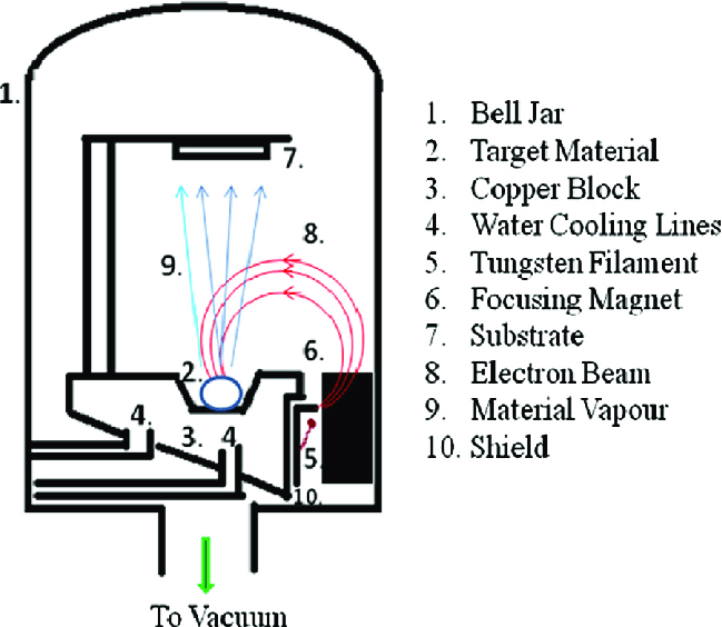
Electron beam deposition is a form of physical vapor deposition (PVD) in which the target anode material is bombarded with a stream of electrons generated by a tungsten filament. Electron beam thin film deposition techniques are widely used in R&D as well as in mass production applications.
Electron beam deposition is performed in a vacuum, typically starting the process at levels below 10-5 Torr. Once a suitable vacuum is reached, a tungsten filament in the electron beam source emits a stream of electrons. This electron beam can be generated in various ways, including thermionic emission, field electron emission, or ion arc source, depending on the design of the source and associated power supply.
In all cases, the negatively charged electrons are attracted to the positively charged anode material. The generated electron beam is accelerated to high kinetic energy and directed towards the material to be deposited on the substrate. This energy is converted into heat by interacting with the atoms of the evaporated material.
The purpose of generating a stream of electrons in an electron beam source is to heat the deposited material to a temperature above a vapor pressure threshold at a given background pressure. The vapor stream is then condensed onto the surface of the substrate.
Deposition Rate
As with all thermal evaporation systems, the electron beam deposition rate depends on the temperature of the material being deposited and the vapor pressure (physical constant) of that material. For elemental materials, there is a fixed vapor pressure for any particular background pressure (vacuum) and material temperature. However, for alloys or composites, there may be different partial pressures associated with each component.
Compared with Sputter Coating
Unlike sputter deposition, where individual atoms arrive at the substrate surface with very high velocity and momentum, the thermally generated vapor stream arrives at the substrate surface at a considerably lower velocity, but a much greater velocity. In other words, e-beam deposition rates can be orders of magnitude greater than sputter deposition rates, making e-beam coatings very beneficial for high volume production or thick film requirements. One disadvantage, however, is that the material tends to condense directly on the substrate surface due to the different kinetic energy of the arriving species during electron beam evaporation than that of the sputtered species. In contrast, atoms of sputtered materials tend to penetrate several atomic layers (or more) to the substrate surface before losing momentum and then establishing cohesive bonds in nucleation structures and film growth. Thus sputtered films tend to provide better adhesion properties than thermally evaporated materials.
For more information, please visit https://www.sputtertargets.net/.