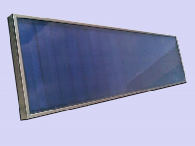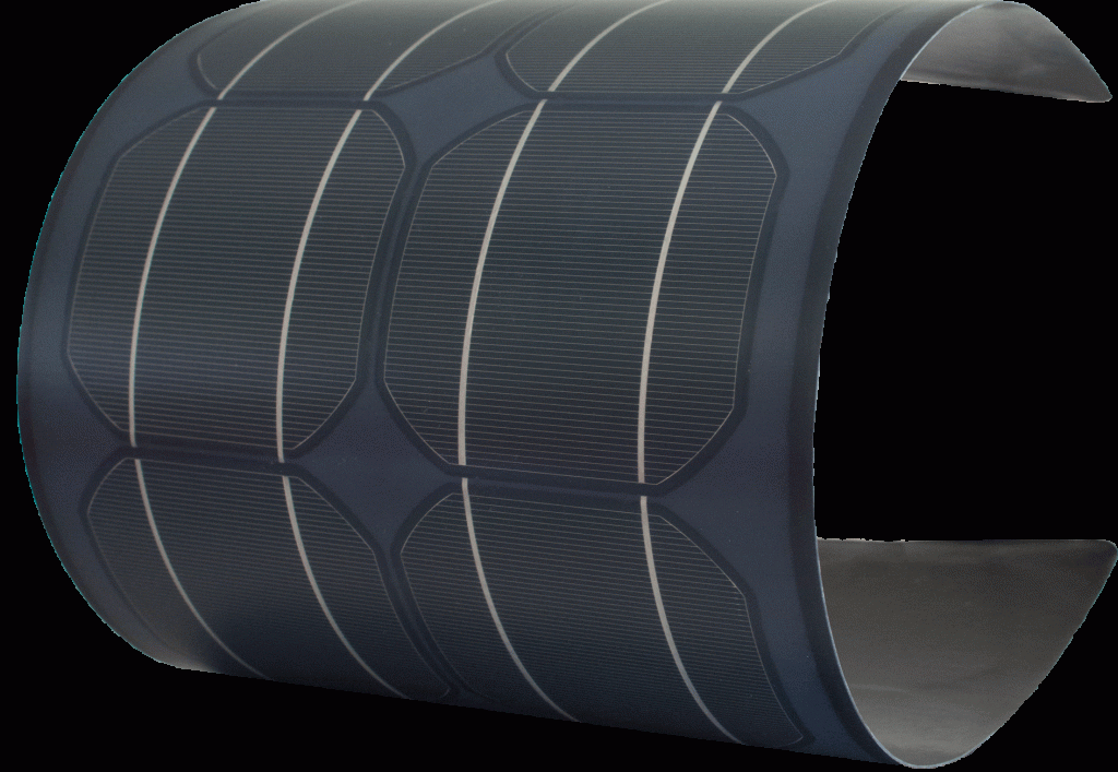
Most modern buildings have begun to use large areas of glass for lighting, and its biggest advantage is that it can bring us brighter light and a wider view. However, since the heat energy transmitted through the glass is much higher than the surrounding walls, the energy consumption of the entire building increases significantly. In order to solve this problem, people have begun to study and apply large-area Low-E glass.
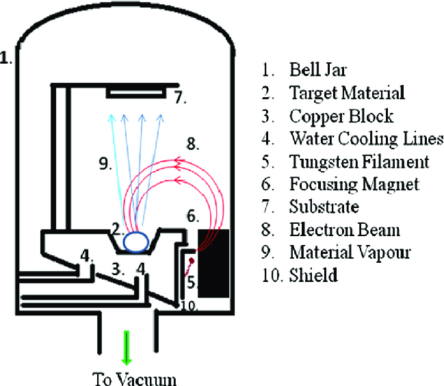
Low-E glass is commonly used in building construction because of its ability to save energy, control light, and for aesthetics. The sputtering target material is one of the essential components for making low-e glass, so this article will introduce 3 factors of target quality that influence large-area coating of low-E glass.
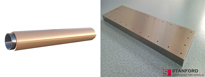
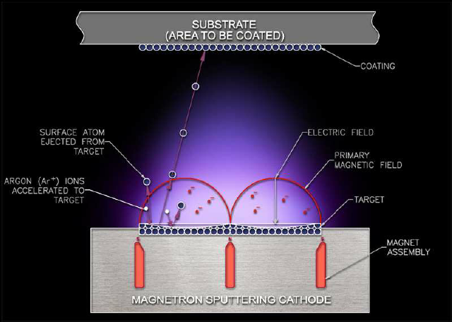
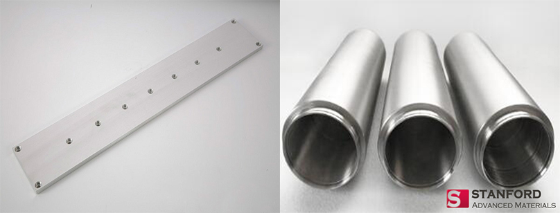
The shape of the target materials
For large-area coating, commonly used targets include planar targets and rotatory targets according to their shapes. The shape of the target affects the stability and film properties of the magnetron sputtering coating, as well as the utilization rate of the target. Therefore, the coating quality and production efficiency can be improved by changing the shape design of the target, and the cost can be saved.
Relative density & porosity of the target
The relative density of the target is the ratio of the actual density to the theoretical density. The theoretical density of a single-component target is the crystal density, and the theoretical density of an alloy or compound target is calculated from the theoretical density of each component and its proportion in the alloy or mixture.
If the target material is loose and porous, it will absorb more impurities and moisture, which are the main pollution sources in the coating process. These impurities will hinder the rapid acquisition of high vacuum, easily lead to electrical discharge during the sputtering process, and even burn out the target. Find high-quality target material here: https://www.sputtertargets.net/
Target grain size and crystallographic direction
For targets of the same composition, the one with the smaller grain size has a faster deposition rate. This is mainly due to the fact that grain boundaries are more vulnerable to attack during the sputtering process, and the more grain boundaries, the faster the film formation.
In addition, the grain size also affects the quality of the film formation. For example, in the production process of Low-E glass, NiCr thin-film is used as the protective layer of the infrared reflection layer Ag, and its quality has a great influence on the coating products. Since the extinction coefficient of the NiCr film is relatively large, it is generally plated very thinly (about 3nm). If the grain size is too large and the sputtering time is short, the compactness of the film will be poor, the protective effect of the Ag layer will be reduced, and the coating product will be oxidized and removed.
Conclusion
The shape of the target mainly affects the utilization rate of the target material, and a reasonable size design can improve the utilization rate of the target material and save costs. The smaller the grain size, the faster the coating rate and the better the uniformity. The higher the purity and density, the lower the porosity, the better the quality of the film formation, and the lower the probability of slag removal by discharge.