Thinning and Coating Process of Mobile Phone Cover Glass

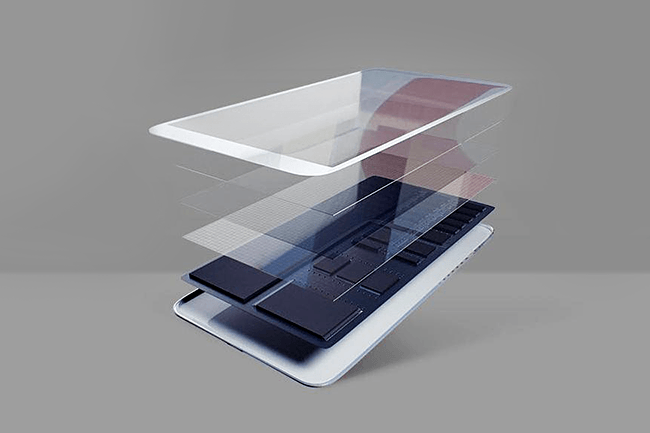
According to the needs of various terminal applications, glass cover panels require various optical glass processing processes such as cutting, edging, drilling, polishing, thinning, chemical strengthening, printing, laser engraving and coating. Today we will introduce the thinning and coating of mobile phone cover glass, which are the most important parts of the whole manufacturing process.

Cover glass thinning process

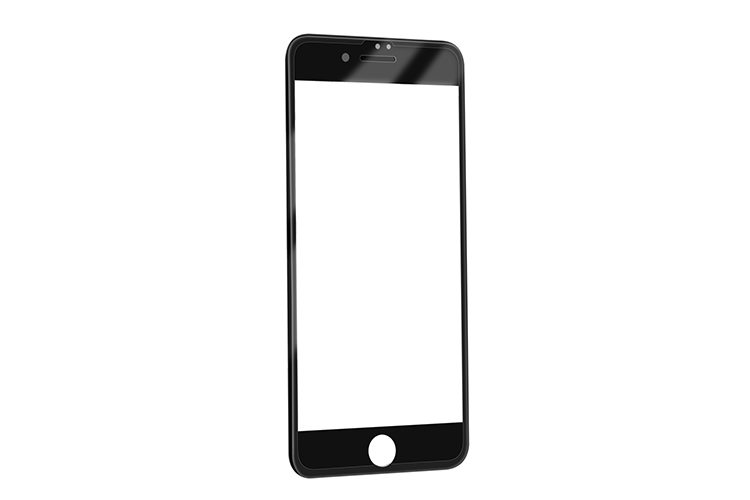
The glass mentioned in this article is not the 3mm, 5mm, 8mm or even 10mm glass for civil use, but the cover glass for electronic products such as smartphones and tablet computers. Among the glasses currently on the market, the thinnest is 0.15 mm. There is a special thinning process that reduces the thickness of the glass.

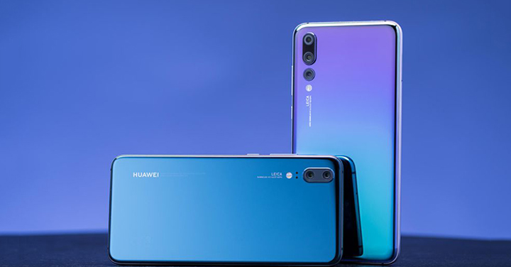
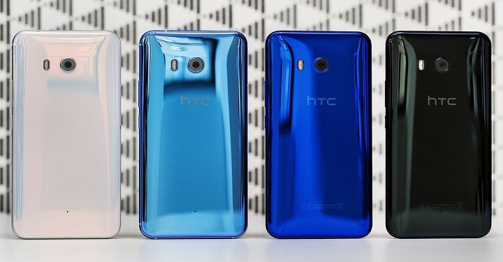
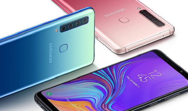
Since Steve Jobs started using Corning Gorilla Glass for his iPhones, there emerges a new component for electronic products—cover glass. At the same time, the pursuit of thinner and lighter in the industry is also urging glass manufacturers to make changes to make thinner cover glass.

iPhone cover glass
iPhone cover glass

Currently, the thinnest glass of gorilla can be made 0.4mm, and the Asahi Glass can make 0.2mm glass. In general, people’s expectations for cover glass are nothing more than two:

1. Reduce the space occupied by the glass.

2. Make the glass cover a certain flexibility.

Mobile phone cover glass thinning process

There are not many processes for glass cover thinning: pre-cleaning—etching and thinning—–secondary cleaning——-grinding (single or double sided)—–post-cleaning—–check the package

Pre-cleaning: Remove the stain on the surface of the glass cover. It is one of the key steps affecting the effect of thinning.

Etching and thinning:  using acid and alkali to etch the glass cover achieve the purpose of thinning. The conditions and parameters (time, potash ratio, temperature, etc.) vary from manufacturer to manufacturer, which is the technical secret of the manufacturer.

Secondary cleaning: Clean the residue of the glass cover.

Grinding: To obtain a bright, flat surface. It is one of the key processes for appearance assurance and thickness tolerance control.

Post-cleaning: Clean the remaining grinding powder.

Check the packaging: The standard for the appearance of the glass is different depending on the requirements of the customer.

Mobile phone cover glass thinning treatment

1, multiple pieces of upright soak

2, waterfall flow processing

3, single piece vertical spray

Cover glass coating process

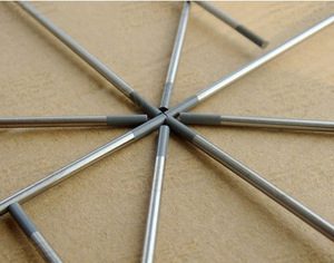
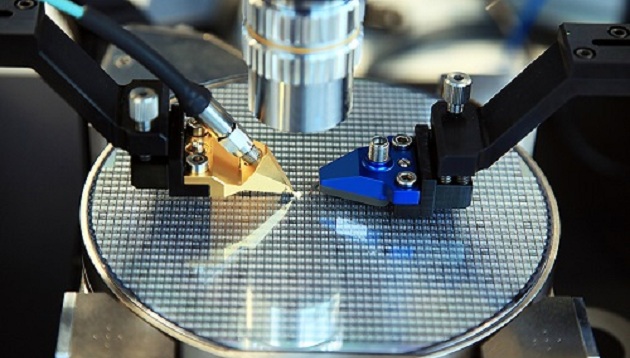
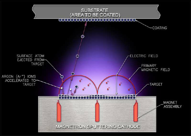
At present, vacuum magnetron sputtering coating technology is a widely used thin film deposition technology. The continuous development of sputtering technology and the exploration of new functional films have enabled the application of magnetron sputtering coating technology to be extended to many productions and scientific research fields.

magnetron sputtering system
magnetron-sputtering-system

magnetron sputtering coating applications

In the field of microelectronics, as a non-thermal coating technology, magnetron sputtering coating technology is mainly applied to materials that are not suitable for chemical vapor deposition or metal organic chemical vapor deposition. Moreover, using magnetron sputtering can obtain a large-area uniform film.

Magnetron sputtering technology is also used in optical films such as antireflection glass, low emissivity glass and transparent conductive glass. In the production of transparent conductive glass, the ITO conductive glass prepared by sputtering has an average transmittance of 90% or more in the visible light range.

In the modern machining industry, the use of magnetron sputtering technology to produce surface functional films, super hard films and self-lubricating films can effectively improve surface hardness, composite toughness, wear resistance and high temperature resistance and chemical stability, thus improve the service life of coated products.

In addition, magnetron sputtering coating technology also plays an important role in the research of high temperature superconducting thin films, ferroelectric thin films, giant magnetoresistive thin films, thin film luminescent materials, solar cells, and memory alloy thin films.

Magnetron sputtering coating advantages

Magnetron sputtering coating technology has become one of the main technologies of the industrial coating due to its remarkable advantages:

(1) Simple operation and easy control. In the coating process, if the sputtering conditions such as working pressure and electric power are relatively stable, the deposition rate is relatively stable.

(2) The deposition rate is high. When depositing most of the metal, especially the high melting point metal and oxide, such as tungsten, aluminum TiO2 and ZrO2 film, it has a high deposition rate.

(3) Low temperature of the substrate. Compared to two-pole sputtering or thermal evaporation, magnetron sputtering reduces the heating of the substrate, which is quite advantageous for achieving the sputter coating of the fabric.

(4) The sputtered film is strong. The sputtered film has excellent adhesion to the substrate and its mechanical strength is also improved.

(5) The sputtered film is dense and uniform. From the photomicrograph, the surface morphology of the sputtered film is fine and uniform.

(6)The sputtered films all have excellent properties. For example, sputtered metal films generally achieve good optical properties, electrical properties, and certain special properties.

(7) Easy to mass produce. The magnetron source can be expanded as required, so large-area coatings are achievable. In addition, sputtering can work continuously, and the coating process is easy to control automatically, so that the industrial assembly line can be realized.

(8) Environmentally friendly. Conventional wet plating produces waste liquid, waste residue, and exhaust gas, causing serious pollution to the environment. The magnetron sputtering coating method has high production efficiency while does not cause environmental pollution.

Please visit https://www.sputtertargets.net/ for more information.

How to make the phone case of gradient color like Huawei P20?

Gradient color is popular in 2018

It’s overwhelming how many smartphone models are currently available on the market today.  However, as for the color of the phone, what get are the same old black, white, silver and gray, in glossy or matte.

Well, recently an exciting new trend has emerged. The Huawei P20 series let people see the optimal color design and professional photography. A few months ago, Huawei launched the P20 in Twilight, and the dual-tone gradient inspired by the Aurora Borealis made people feel excited.

Huawei P20
Huawei P20

Before that, HTC also introduced the two-tone gradient scheme. Although it does not offer the popular Twilight color scheme, it does bring us a few appealing options with its latest flagship device.

HTC U11
HTC U11

Samsung has also jumped on board the gradient crazy. The Korean tech giant has unveiled a new version of its Galaxy A9 Star in China which features a sleek purple gradient.

Galaxy A9 Star2
Galaxy A9 Star2

Well, these are just a few examples to show that gradient color is the fashion of the year 2018. Are you curious about how to achieve this kind of gradient color? Is it difficult?

Film coating-Physical vapor deposition

Actually, all the color of the shell is about film coating. A cellphone is made from a variety of metals, with the most common being aluminum alloys, lightweight materials commonly found in the phone case. And the film coating is to apply a colored film on the phone case.

Physical vapor deposition is the most widely used film coating technology. Under vacuum conditions, the surface of the material (usually referred to as the sputtering targets or evaporating pellets) is vaporized into gaseous atoms by physical methods, and is then deposited on the surface of the substrate to form a thin film. The main methods of physical vapor deposition include vacuum evaporation, sputtering coating, plasma coating, ion plating, and molecular beam epitaxy.

How to coat the gradient color

PVD can coat gold, brass, rose gold, silver white, black, smoky, copper, brown, purple, blue, burgundy, bronze and other colors on stainless steel, copper, zinc alloy and other metals. There are many choices and the price is affordable, compared to pure gold or other pure metals. (PVD Coating Materials.pdf) You can refer to our previous article for more information: Introduction to PVD Coatings.

By controlling the parameters of different targets and thickness of the deposited film, the film exhibits different colors (the gradation colors mentioned above) under the reflection, refraction and interference of light. Specifically, in the plating furnace space, bombard a specific sputtering target with ultra-high speed electrons; use a certain mask to cover a part of the ion cloud so that only the other part of the ion cloud can be attached to the substrate and forms a very thin layer of nano-plating; control the thickness of the coating to form a nanometer thickness difference; then spray the background color.

For more information, please visit https://www.sputtertargets.net/.

Year in Review: 2018 Top Posts Collection

Happy New Year in 2019! We are very happy with your company and encouragement that push us to insist on updating every week. On the occasion of the arrival of 2019, let us summarize the Top Posts in 2018 for you.

Metal History

“Metal History” is a popular column we have opened this year, aiming at introducing the discovery of different kinds of metals. Among them, the Top 3 posts in this column are as follows:

How was titanium discovered? | History of Titanium

Titanium is a metal element that is known as “space metal” because of its light weight, high strength and good corrosion resistance. The most common compound of titanium is titanium dioxide, and other compounds include titanium tetrachloride and titanium trichloride. Click the title of the article to know more.

Discovery and development of tungsten | History of Tungsten

The history of tungsten dates back to the 17th century. At that time, miners in the Erzgebirge Mountains of Saxony, Germany, noticed that some of the ore would interfere with the reduction of cassiterite and produce slag. The miners gave the mines some German nicknames: “wolfert” and “wolfrahm”. Click the title of the article to know more.

How was cerium discovered? | History of Cerium

Cerium is the most abundant rare earth elements. It is a silvery gray active metal, whose powder is easily oxidized in the air and soluble in acid. Cerium has been widely used in the automotive industry as a catalyst to reduce emission, and in glass industry as glass polishing materials. Cerium sputtering target is an important material in optical coating. Click the title of the article to know more. Click the title of the article to know more.

Metal Materials Application

Apart from history, we also introduce the multiple applications of these metal materials. Among them, the Top 3 posts in this column are as follows:

Molybdenum Target Mammography Detection

At present, molybdenum target mammography is considered the recommended breast screening examinations for women’s breast cancer, one of the major causes of deaths among women, affects about 12% of women around the world. Click the title of the article to know more.

Application of titanium and titanium alloys in medical field

Titanium is an ideal medical metal material and can be used as an implant for the human body. Titanium alloy has been widely used in the medical field and has become the material of choice for medical products. Click the title of the article to know more.

A short analysis of sputtering targets for semiconductor application

Semiconductors have high requirements for the quality and purity of the sputtering materials, which explains why the price of anelva targets is relatively high. Click the title of the article to know more.

Sputtering Targets

Sputtering Target is the consistent keyword of our website, and thus we have shared many useful information about some specific type of sputtering targets. Our intention is to help you better understand these materials—their properties, applications, developing prospect and so on. And the followings are the posts you really have to read. Among them, the Top 3 posts in this column are as follows:

PVD vs. CVD: What’s the difference?

In recent years, physical vapor deposition (PVD) and chemical vapor deposition (PVD) have wide applications in various industries to increase the hardness of tools and molds or apply beautiful colors to the products. Thus these two methods are considered as the most attractive surface coating technologies. Click the title of the article to know more.

What is the Indium Bonding for Sputtering Target?

The term “indium bonding” in thin film coating industry, simply speaking, refers to bond two (or more) sputtering targets with indium (In), or one (or more) with indium plate together. Click the title of the article to know more.

What is Target Poisoning in Sputtering Deposition?

At some stage in the sputtering deposition, positive ions are continuously amassed on the surface of the sputtering target. Due to the fact that those fantastic ions aren’t neutralized, the negative bias of the target surface gradually decreases, and progressively the normal operation can not be completed. This is the target poisoning phenomenon. Click the title of the article to know more.

Glad you are part of SAM’s 2018. Next year, please continue following us and we promise to give you more valuable information! Also, you can visit our official website https://www.sputtertargets.net/ for more information.

How was Silicon discovered? | History of Silicon

Silicon

Discovery of Silicon

In 1787, the French chemist Antoine-Laurent de Lavoisier first discovered the silicon present in rocks. In 1800, silicon was mistaken by Sir Humphry Davy as a compound. In 1811, French chemists Joseph Louis Gay-Lussac and Louis Jacques Thénard probably prepared impure amorphous Silicon by heating potassium with silicon tetrafluoride. They later named it silicon according to the Latin silex (meteorite).

Until 1823, silicon was first discovered in the form of a metal element by the Swedish chemist Jöns Jacob Berzelius. One year later, he extracted amorphous silicon in much the same way as Gay-Lussac, and then purified the elemental silicon by repeated cleaning; in the same year, he heated the silicon oxide powder and the mixture of iron and carbon at a high temperature and obtain the iron silicide.

In order to extract pure silicon, Berzelius dry-fired the silicon-fluorine-calcium compound, hydrolyzed the obtained solid, and manage to obtain the pure silicon. In 1824, in Stockholm, Berzelius obtained relatively pure silicon powder by heating potassium fluorosilicate and potassium. Therefore, it is agreed that the honor of discovering silicon belongs to Berzelius.

Properties of Silicon

Symbol: Si
Atomic Number: 14
Atomic Weight: 28.09
Element Category: metalloid
Color: dark gray with a bluish tinge
Density: 2328.3 kg/m³
Hardness: 6.5
Proportion in Earth’s Crust: 25.7%
Other Names: Silicium, Silicio

Application of Silicon

High-purity monocrystalline silicon is an important semiconductor material that can be used as a solar cell to convert radiant energy into electrical energy, which is a promising material in the development of energy.

Silicon can also be made into cermet composites, which are resistant to high temperatures, toughness, and can be cut. They not only inherit the respective advantages of metals and ceramics, but also make up for the inherent defects of both, and can be applied to weapons manufacturing and aerospace.

Pure silica can be used to draw high transparency glass fiber for optical fiber communication, which is the latest modern communication means.

Please visit https://www.sputtertargets.net/ for more information.

What is the Indium Bonding for Sputtering Target?

Read more: What Is Indium Bonding for Sputtering Target?

The term “indium bonding” in the thin film coating industry, simply speaking, refers to bonding two (or more) sputtering targets with indium (In), or one (or more) indium plates together.

Indium

Indium can be uniquely used in lower temperature solders, is one of the softest materials. Indium is preferred for target bonding because of its excellent thermal conductivity of all available bonds. In addition, indium is the most efficient material at drawing heat away from the sputtering target. Most materials can be indium bonded and there are just a few exceptions.

Apart from indium bonding, indium is also popular for a variety of uses and purposes, such as creating alloys, photoconductors, and thermistors.

Indium bond

Sputtering targets can be cracked, warped, or damaged due to inadequate cooling, low hardness, or other reasons. From this point of view, although target bonding does generate a fee, it can well protect your target from damage. It is especially true for those less-strong target materials and precious metal materials.

Elastomer is an alternative bonding method that touts a higher temperature capability over the indium bond. Elastomer bonds are recommended when you are consistently melting indium bonds. We also recommend elastomer bonding for low melting point target materials, as well as, temperature-sensitive compounds and targets that have either low density or are especially fragile.

indium target bonding

Indium bonding is preferred in applications where:

Cryogenic stability is needed

Sealing requires high levels of hermeticity

Maximum thermal transfer is required

Bonding to not-metallic surfaces

Flux cannot be used

Backing plates

OFHC Copper Backing Plate is another well-known backing plate. It is frequently used to bond ceramic targets because of its non-magnetism and low coefficient of thermal expansion. This metal has good electrical and thermal characteristics while also being easy to machine, easy to soften, and readily available at a low cost. Copper backing plates can be re-used, with care, 20 or more times.

A molybdenum plate is usually used to substitute copper plate if copper is not appropriate for the application. For instance, the coefficient of expansion for copper is mismatched with some ceramics. And for high-temperature bonding, copper may also oxidize badly or warp. In these conditions, molybdenum is a more suitable material.

SAM Sputter Target

If you are looking for an indium bonding manufacturer, SAM is undoubtedly your best choice. Stanford Advanced Materials is devoted to machining standard backing plates and working together with the Taiwan Bonding Company for providing bonding services. For questions about target bonding materials, methods, and services, please see our listing of frequently asked questions (FAQs).

Related blog: When do you need target bonding?

Molybdenum Target Mammography Detection

Breast cancer, one of the major causes of deaths among women, affects about 12% of women around the world. According to research surveys, the smaller the breast cancer is when it is detected, the less the possibility of death. This requires that women should go over the medical body check regularly to decrease the risk of breast cancer. At present, molybdenum target mammography is considered the recommended breast screening examinations for women’s breast cancer.

What is the Breast Cancer?

Breast cancer is caused by the development of malignant cells in the breast. It is a sign of breast cancer when cells in the breast begin to grow out of control, and these cells usually result in forming a tumor.

Breast Cancer
Breast Cancer


Breast cancer itself is not a fatal disease because the breast is not an indispensable organ for maintaining human life. However, if the malignant cells spread to other important parts of the human body, such as the heart, the liver, and kidney, breast cancer may lead to death.

Breast cancer occurs almost entirely in women, but men can get breast cancer, too. And it is closely related to age—only 5% of all breast cancers occurring in women under 40 years old.

What is Molybdenum target mammography?

Molybdenum target, or molybdenum sputtering target, is known as the materials in physical vapor deposition for film coating.

Molybdenum target mammography is another important application of Molybdenum target. It is a non-invasive method to test breast diseases such as breast mass and calcification. From the viewpoint of techniques, it is a digital imaging technology that combines traditional radiology technology with modern computer technology that transforms the X-ray image into a digital image that can be quantized. Molybdenum target mammography enables radiologists to find suspicious malignant lesions in mammography easier. Thus, it has been used as a routine examination to reduce the risk of breast cancer.

Molybdenum target mammography
Molybdenum Target Mammography

Why is Molybdenum target mammography beneficial?

Molybdenum target mammography is currently the primary choice for the diagnosis of breast disease. It is an easy and non-invasive method of examination which can accurately reflect the condition of the entire breast. What’s more, it can be used to observe the breast disease caused by various factors and the results are relatively reliable. With the help of Molybdenum inspection, some precancerous lesions can be found and can be followed up for observation. So it is beneficial for women’s health.

Above information is from SAM Sputter Target, a global sputtering targets manufacturer specialized in Molybdenum target.

How was cerium discovered? | History of Cerium

Cerium is the most abundant rare earth elements. It is a silvery gray active metal, whose powder is easily oxidized in the air and soluble in acid. Cerium has been widely used in the automotive industry as a catalyst to reduce emission, and in glass industry as glass polishing materials. Cerium sputtering target is an important material in optical coating.

Discovery History

In 1803, when the German chemist Martin Heinrich Klaproth analyzed an ore, he determined the existence of a new metal oxide and called it ochra (ocha-colored soil). and the ore ochroite because it appears to be ochre when burning.

In the same year, the Swedish chemist Jöns Jakob Berzelius and the Swedish mineralogist Wilhelm Hisinger also analyzed the same new metal oxide, which is different from yttrium. Yttrium is dissolved in ammonium carbonate solution and appears red when burning on gas flame. However, this metal oxide is insoluble in ammonium carbonate solution and does not exhibit characteristic flame color when burning.

The ore is thus called ceria (bauxite), and the element is named cerium to commemorate the discovery of an asteroid, Ceres.

Discovery of cerium

Three Early Applications of Cerium

Carl F. Auer von Welsbach
Carl Auer von Welsbach

Eighty-three years after the discovery of “cerium”, in 1886, the Austrian Carl Auer von Welsbach found the first application of cerium (also rare earth) as a luminescent enhancer for steam hoods. He found that heating 99% thorium oxide and 1% cerium oxide would give off a strong light, so cerium used in coal gas lamp gauze can greatly increase the brightness of the gas lamp. The gas lamps in Europe, where electric lights were not yet popular, were the main source of lighting and were essential for industrial production, commerce, and life.

After the First World War, electric lights gradually replaced gas lamps, but cerium continued to open up new applications. In 1903, Welsbach once again discovered the second largest use of cerium. He found that cerium iron alloys can generate sparks under mechanical friction and therefore can be used to make flints. This classic use of cerium has been around for 100 years. Everyone who smokes knows that a lighter uses a flintstone, but many people they that it is cerium that brings fire to people.

cerium arc carbon rods

In 1910, the third important application of cerium was discovered for arc carbon rods in searchlights and film projectors. Similar to the steam cover, cerium can improve the efficiency of visible light conversion. Searchlights were once an important tool in war air defense. Arc carbon rods have also been an indispensable source of light for filming.

Modern Applications of Cerium

Since the 1930s, cerium oxide has been used as a glass decolorizer, clarifier, colorant, and abrasive polishing agent.

As a chemical decolorizer and clarifier, cerium oxide can replace the highly toxic white magnetic (oxidation) to reduce operational and environmental pollution.

The use of cerium titanium yellow pigment as a glass colorant produces a beautiful bright yellow art glass.

Cerium oxide as a main component to manufacture various specifications of polishing powder has completely replaced iron red polishing powder, greatly improving polishing efficiency and polishing quality.

As a glass additive, cerium can absorb ultraviolet light and infrared rays and thus has been widely used in automotive glass. It not only protects against UV rays but also reduces the temperature inside the car, thus saving air conditioning power.

cerium polishing powder

This history column aims at introducing the history of different metal elements. If you are a metal lover or history lover, you can follow our website. For previous posts of metal history, you can look them up in the “history” category.

Please visit https://www.sputtertargets.net/ for more information.

Application of titanium and titanium alloys in medical field

Titanium is an ideal medical metal material and can be used as an implant for human body. Titanium alloy has been widely used in the medical field and has become the material of choice for medical products such as artificial joints, bone trauma, spinal orthopedic internal fixation systems, dental implants, artificial heart valves, interventional cardiovascular stents, and surgical instruments.

Application of titanium alloy in facial treatment

When the human face is severely damaged, local tissue repair should be treated by surgical implantation. Titanium alloy has good biocompatibility and required strength, so it is an ideal material for facial tissue repair. The skull bracket made of pure titanium mesh has been widely used in the reconstruction of the humerus and has achieved good clinical results.

titanium mesh
titanium mesh

Application of titanium in the pharmaceutical industry

SAM®Titanium is mainly used in the pharmaceutical industry for making containers, reactors, and heaters. Equipment used in the production of pharmaceuticals is often exposed to inorganic acids, organic acids, and salts, such as hydrochloric acid, nitric acid, and sulfuric acid. Therefore, these devices are easily damaged by long-term corrosion. On the other hand, steel equipment will introduce iron ions that affect product quality.

These problems can be solved with titanium equipment. For example, a penicillin esterification kettle, a saccharification tank, a chloramphenicol thin film evaporator, a dimethyl sulfate cooler, a chemical liquid filter, all have precedents for selecting a titanium material.

Application of titanium in medical devices

In the history of the development of surgical instruments, the first generation of surgical instruments was mostly made of carbon steel, which was eliminated because the performance of carbon steel instruments after electroplating did not meet the clinical requirements. The second generation is austenitic, ferritic and martensitic stainless steel surgical instruments. However, due to the toxicity of chromium in the stainless steel composition, the chrome-plated layer has a certain influence on the human body. Therefore, the third generation–titanium surgical instrument appeared.

titanium surgical blades

The lightweight and high strength of titanium make it particularly suitable for microsurgery. Titanium has the advantages of corrosion resistance, good elasticity, and no deformation; even after repeated cleaning and disinfection, the surface quality of titanium is not affected; titanium is non-magnetic and does not pose a threat to tiny, sensitive implanted electronic devices. These advantages make the application of titanium surgical instruments more and more extensive. At present, titanium has been used to make surgical blades, hemostats, scissors, electric drills, tweezers and so on.

Application of titanium and titanium alloys in dentistry

Metals used in dental surgery began with amalgams and metal crowns in the 1920s. In the 1960s, gold, silver, and palladium alloys were mainly used. After the 1970s, stainless steel became the most commonly used material for permanent and detachable instruments for orthodontics. In the 1990s, titanium casting technology was promoted and applied.

titanium dental implant

Titanium has the characteristics of high dimensional accuracy, no bubbles, and shrinkage holes. Among the metal materials used for hard tissue repair in the human body, the elastic modulus of titanium is closest to human tissue, which can reduce the mechanical incompatibility between the metal implant and the bone tissue.

Please visit https://www.sputtertargets.net/ for more information.

Quick link to related titanium products:

Titanium (Ti) Sputtering Target

Planar Titanium (Ti) Sputtering Target

Rotatory Titanium (Ti) Sputtering Target

A short analysis of sputtering targets for semiconductor application

Semiconductors have high requirements for the quality and purity of the sputtering materials, which explains why the price of anelva  targets is relatively high.

Undoubtedly, sputtering targets are the most important raw materials in current semiconductor manufacturing processes. Their quality and purity play a key role in the subsequent production quality of the semiconductor industry chain. And anelva targets refer to those sputtering targets used in the semiconductor industry.

Application requirements

Semiconductors have high requirements for the quality and purity of the sputtering materials, which explains why the price of anelva  targets is relatively high. In the semiconductor manufacturing process, if the impurity content of the sputtering target is too high, the formed film cannot achieve the required electrical properties, and it is liable to cause short circuit or damage of the circuit, which will seriously affect the performance of the film.

Therefore, when purchasing semiconductor targets, be sure to find a reliable sputtering targets manufacturers for high-quality & high-purity sputtering targets.

blue computer circuit board closeup , semiconductor industry

Market Size

With the rapid development of terminal applications such as consumer electronics, the market sales of high-purity sputtering targets are expanding.

According to statistics, in 2015, the global high-purity sputtering target market sales reached 9.48 billion US dollars, of which, the semiconductor sputtering target market sales of 1.14 billion US dollars. It is estimated that in the next five years, the market size of the world’s sputtering targets will exceed 16 billion US dollars, and the CAGR (Compound Annual Growth rate) of the high-purity sputtering target market will reach 13%.

According to statistics from WSTS (World Semiconductor Trade Statistics), the global target market is expected to grow at the same rate as 2017 (13%). In 2016, the global sputtering target market capacity was US$11.36 billion, an increase of 20% compared to US$9.48 billion in 2015. It can be inferred that the market size of the global high-purity sputtering target in 2018 is about 14.5 billion US dollars.

Stanford Advanced Materials (SAM) Corporation is a global supplier of sputtering targets such as metals, alloys, oxides and ceramic materials, which are widely used in multiple industries. Please visit https://www.sputtertargets.net/ for more information.

Application of molybdenum in metal smelting

Compared to metals such as titanium, aluminum and platinum, molybdenum does not seem to be as famous, but it is also a very widely used metal in our life. So in the next few weeks, SAM Sputter Targets will introduce different applications of molybdenum. If you are interested in metals, please follow us for subsequent updates. Today we will first introduce the application of molybdenum in metal smelting.

Molybdenum
Molybdenum

Steel

The main use of molybdenum is to produce various types of steel and alloys. The addition of molybdenum (mainly in the form of ferromolybdenum, molybdenum oxide and calcium molybdate) to a range of steels such as structural steel, spring steel, bearing steel, tool steel, stainless steel and magnetic steel can significantly improve the properties of steel. Molybdenum improves the hardenability, toughness and heat strength of steel and prevents temper brittleness. Molybdenum also improves the corrosion resistance of steel to certain media so that it does not pitting. The addition of molybdenum to the cast iron enhances the strength and wear resistance of the cast iron.

Continue reading “Application of molybdenum in metal smelting”