Introduction to the Process and Steps of Evaporation Coating

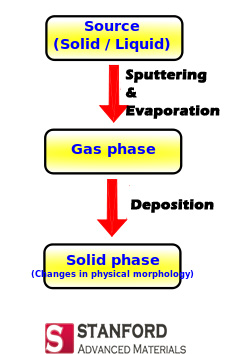
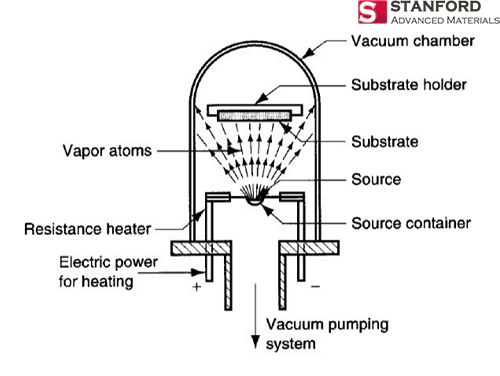
The basic process flow for evaporation coating is:

Preparation before coating→ vacuum→ ion bombardment→ baking→ premelting→ evaporation→ removing parts→ film surface treatment→ finished product

1. Preparation before coating

The process includes vacuum chamber coating part cleaning, evaporation source making and cleaning, installation of evaporation source and evaporation materials.

The amount of bonding between the film layer and the surface of substrate is an important indicator of product quality. It is determined by many factors, and the surface treatment before coating is one of the most basic factors. If there is grease on the surface of the coating part, adsorbing water, dust, etc., it will reduce the bonding force of the film layer and affect the surface roughness. Cleaning is generally done by several methods: chemical degreasing, electrostatic dedusting and primer application.

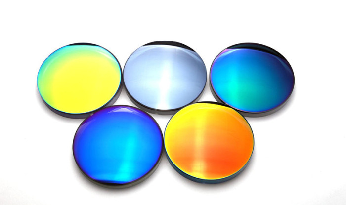
According to the requirements of the product and the material of the coating parts, selecting the appropriate evaporation material is the basic condition for obtaining a high-quality film layer. For different evaporation materials, the corresponding evaporation source and the evaporation method should be selected.

The basic principle of selecting metal evaporation materials is: good thermal stability and chemical stability, high mechanical strength, low internal stress, and certain toughness, good bonding with primer, high reflectivity, and small gas release in vacuum; the material source is wide, the price is low, and it has a corresponding evaporation source.
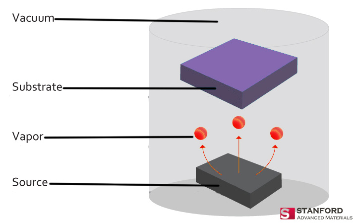
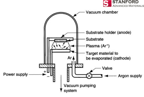
2. Vacuum step

Open the cooling water valve, adjust to the required water pressure, turn on the main power supply, close the atmospheric valve leading to the vacuum chamber, close the pipeline valve, start the mechanical pump power supply, and open the pre-vacuum valve; At this time, the vacuum chamber is evacuated using a diffusion pump or a mechanical pump, and baking, pre-melting, and evaporation are performed when the degree of vacuum reaches a certain value.
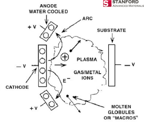
3. Ion bombardment

In the glow discharge, the ion bombardment electrons obtain a high speed, and the negative charge is rapidly generated around the substrate due to the large mobility of the electron. Under the action of the negative charge attraction, the positive ion bombards the surface of the coating part, and the substrate. There is energy exchange on the surface, and a chemical reaction occurs between the adsorption layer of the coating member and the active gas to achieve the effect of cleaning the surface.
The conditions of ion bombardment are that the residual gas pressure is stable at 0.13~13Pa, the voltage is 1.5~10kV, and the time is 5~60min.

4. Baking

It can accelerate the rapid escape of the gas adsorbed by the coating parts or the clamp, which is beneficial to improve the vacuum degree and the film bonding force. When baking, it should be noted that the non-metal baking temperature is lower than the hot deformation temperature of the coating part by 20~30 °C, and the metal baking is generally not more than 200 °C.

5. Pre-melting

This step can remove the low melting point impurities in the evaporation material and the gas adsorbed in the evaporation source and the evaporation material, which is favorable for the smooth progress of evaporation. The pre-melted vacuum is generally 6.6 x 10⁻³ Pa. For materials with high hygroscopicity, it should be pre-melted repeatedly. The overall requirement is that the vacuum does not drop as the evaporating material warms to the evaporating temperature.

6. Evaporation

Evaporation technology has a great impact on film quality. There are different requirements for general metals, special metals and compound evaporating pellets. For example, some metal particles need to be evaporated quickly, while others are not suitable. The heating method and the shape of the evaporation source should also be different depending on the evaporation material.

Please visit https://www.sputtertargets.net/by-evaporation-materials.html for more information.

Physical Vapor Deposition: Sputter Coating & Evaporation

Physical vapor deposition processes use vacuum technology to create a sub-atmospheric pressure environment and an atomic or molecular condensable vapor source (from a solid or liquid surface) to deposit thin films and coatings. Sputtering deposition and vacuum evaporation are among the more well known.

physical vapor deposition sputtering evaporation

Sputtering deposition

The sputtering deposition is an etching process that alters the physical properties of a surface. In this process, a gas plasma discharge is set up between two electrodes: a cathode plating material (the sputter coater targets) and an anode material (the substrate). The film made by sputter coating are thin, ranging from 0.00005 – 0.01 mm. Chromium, titanium, aluminum, copper, molybdenum, tungsten, gold, and silver are typical sputter coating targets.

Sputter coated films are used routinely in decorative applications such as watchbands, eyeglasses, and jewelry. Also, the electronics industry relies on heavily sputtered coatings and films, such as thin film wiring on chips and recording heads as well as magnetic and magneto-optic recording media. Companies also use sputter deposition to produce reflective films for large pieces of architectural glass used in the automotive industry. Compared to other deposition processes, sputter deposition is relatively inexpensive.

vacuum coating

Vacuum Evaporation

The vacuum evaporation is a process of reducing the wastewater volume through a method that consists of concentrating a solution by eliminating the solvent by boiling. In this case, it is performed at a pressure lower than atmospheric pressure. Thus, the boiling temperature is much lower than that at atmospheric pressure, thereby resulting in notable energy savings. The basic components of this process consist of: evaporation pellets,  heat-exchanger, vacuum, vapor separator, and condenser.

Vacuum evaporation is used in the semiconductor, microelectronics, and optical industries and in this context is a process of depositing thin films of material onto surfaces. High-purity films can be obtained from a source evaporation material with high purity. The source of the material that is going to be vaporized onto the substrate can be a solid in any shape or form (usually pellets). The versatility of this method trumps other deposition processes. Also, when the deposition is not desired, masks are utilized to define the areas on the substrate for control purposes.

Information from Stanford Advanced Materials. Please visit https://www.sputtertargets.net/ for more information.

Working Mechanism of Pulsed Laser Deposition

Pulsed laser deposition (PLD) is a physical vapor deposition (PVD) technique where a high-power pulsed laser beam is focused inside a vacuum chamber to strike a target of the material that is to be deposited.  Although the equipment of pulsed laser deposition (PLD) system is simple, its working mechanism is related to many complicated physical phenomena. It includes all physical interactions between the laser and the substance when the high-energy pulsed radiation strikes the solid sputtering target, the formation of plasma plumes and the transfer of the molten material through the plasma plume to the surface of the heated substrate. Therefore, PLD can generally be divided into the following three stages:

Interaction between laser radiation and the sputtering target

In this stage, the laser beam is focused on the surface of the target materials. When sufficient high energy flux and short pulse width are achieved, all elements of the target surface are rapidly heated to the evaporation temperature. At this point, the material in the target will be sputtered from the target. The instantaneous melting rate of the target is highly dependent on the flow of laser light onto the target. The melting mechanism involves many complex physical phenomena such as collisions, heat, excitation with electrons, delamination, and fluid mechanics.

Dynamics of molten matter

In the second stage, according to the law of aerodynamics, the sputtered particles have a tendency to move toward the substrate. The space thickness varies with the function cosn θ, and n>>1. The area of the laser spot and the temperature of the plasma have an important influence on the uniformity of the deposited film. The distance between the target and the substrate is another factor that affects the angular extent of the molten material. It has also been found that placing a baffle close to the substrate narrows the angular extent.

Deposition of molten material on the substrate

The third stage is the key to determining the quality of the film. The high-energy nuclides emitted hit the surface of the substrate and may cause various damages to the substrate. The high energy nuclide sputters some of the atoms on the surface, and a collision zone is established between the incident stream and the sputtered atoms. The film is formed immediately after the formation of this thermal energy zone (collision zone), which is the best place to condense particles. As long as the condensation rate is higher than the release rate of the sputtered particles, the heat balance condition can be quickly reached, and the film can be formed on the surface of the substrate due to the weakened flow of the molten particles.

The original text is from https://samsputtertargets.blogspot.com/.

Please visit https://www.sputtertargets.net/ for more information.

Thinning and Coating Process of Mobile Phone Cover Glass

According to the needs of various terminal applications, glass cover panels require various optical glass processing processes such as cutting, edging, drilling, polishing, thinning, chemical strengthening, printing, laser engraving and coating. Today we will introduce the thinning and coating of mobile phone cover glass, which are the most important parts of the whole manufacturing process.

Cover glass thinning process

The glass mentioned in this article is not the 3mm, 5mm, 8mm or even 10mm glass for civil use, but the cover glass for electronic products such as smartphones and tablet computers. Among the glasses currently on the market, the thinnest is 0.15 mm. There is a special thinning process that reduces the thickness of the glass.

Since Steve Jobs started using Corning Gorilla Glass for his iPhones, there emerges a new component for electronic products—cover glass. At the same time, the pursuit of thinner and lighter in the industry is also urging glass manufacturers to make changes to make thinner cover glass.

iPhone cover glass
iPhone cover glass

Currently, the thinnest glass of gorilla can be made 0.4mm, and the Asahi Glass can make 0.2mm glass. In general, people’s expectations for cover glass are nothing more than two:

1. Reduce the space occupied by the glass.

2. Make the glass cover a certain flexibility.

Mobile phone cover glass thinning process

There are not many processes for glass cover thinning: pre-cleaning—etching and thinning—–secondary cleaning——-grinding (single or double sided)—–post-cleaning—–check the package

Pre-cleaning: Remove the stain on the surface of the glass cover. It is one of the key steps affecting the effect of thinning.

Etching and thinning:  using acid and alkali to etch the glass cover achieve the purpose of thinning. The conditions and parameters (time, potash ratio, temperature, etc.) vary from manufacturer to manufacturer, which is the technical secret of the manufacturer.

Secondary cleaning: Clean the residue of the glass cover.

Grinding: To obtain a bright, flat surface. It is one of the key processes for appearance assurance and thickness tolerance control.

Post-cleaning: Clean the remaining grinding powder.

Check the packaging: The standard for the appearance of the glass is different depending on the requirements of the customer.

Mobile phone cover glass thinning treatment

1, multiple pieces of upright soak

2, waterfall flow processing

3, single piece vertical spray

Cover glass coating process

At present, vacuum magnetron sputtering coating technology is a widely used thin film deposition technology. The continuous development of sputtering technology and the exploration of new functional films have enabled the application of magnetron sputtering coating technology to be extended to many productions and scientific research fields.

magnetron sputtering system
magnetron-sputtering-system

magnetron sputtering coating applications

In the field of microelectronics, as a non-thermal coating technology, magnetron sputtering coating technology is mainly applied to materials that are not suitable for chemical vapor deposition or metal organic chemical vapor deposition. Moreover, using magnetron sputtering can obtain a large-area uniform film.

Magnetron sputtering technology is also used in optical films such as antireflection glass, low emissivity glass and transparent conductive glass. In the production of transparent conductive glass, the ITO conductive glass prepared by sputtering has an average transmittance of 90% or more in the visible light range.

In the modern machining industry, the use of magnetron sputtering technology to produce surface functional films, super hard films and self-lubricating films can effectively improve surface hardness, composite toughness, wear resistance and high temperature resistance and chemical stability, thus improve the service life of coated products.

In addition, magnetron sputtering coating technology also plays an important role in the research of high temperature superconducting thin films, ferroelectric thin films, giant magnetoresistive thin films, thin film luminescent materials, solar cells, and memory alloy thin films.

Magnetron sputtering coating advantages

Magnetron sputtering coating technology has become one of the main technologies of the industrial coating due to its remarkable advantages:

(1) Simple operation and easy control. In the coating process, if the sputtering conditions such as working pressure and electric power are relatively stable, the deposition rate is relatively stable.

(2) The deposition rate is high. When depositing most of the metal, especially the high melting point metal and oxide, such as tungsten, aluminum TiO2 and ZrO2 film, it has a high deposition rate.

(3) Low temperature of the substrate. Compared to two-pole sputtering or thermal evaporation, magnetron sputtering reduces the heating of the substrate, which is quite advantageous for achieving the sputter coating of the fabric.

(4) The sputtered film is strong. The sputtered film has excellent adhesion to the substrate and its mechanical strength is also improved.

(5) The sputtered film is dense and uniform. From the photomicrograph, the surface morphology of the sputtered film is fine and uniform.

(6)The sputtered films all have excellent properties. For example, sputtered metal films generally achieve good optical properties, electrical properties, and certain special properties.

(7) Easy to mass produce. The magnetron source can be expanded as required, so large-area coatings are achievable. In addition, sputtering can work continuously, and the coating process is easy to control automatically, so that the industrial assembly line can be realized.

(8) Environmentally friendly. Conventional wet plating produces waste liquid, waste residue, and exhaust gas, causing serious pollution to the environment. The magnetron sputtering coating method has high production efficiency while does not cause environmental pollution.

Please visit https://www.sputtertargets.net/ for more information.

How to make the phone case of gradient color like Huawei P20?

Gradient color is popular in 2018

It’s overwhelming how many smartphone models are currently available on the market today.  However, as for the color of the phone, what get are the same old black, white, silver and gray, in glossy or matte.

Well, recently an exciting new trend has emerged. The Huawei P20 series let people see the optimal color design and professional photography. A few months ago, Huawei launched the P20 in Twilight, and the dual-tone gradient inspired by the Aurora Borealis made people feel excited.

Huawei P20
Huawei P20

Before that, HTC also introduced the two-tone gradient scheme. Although it does not offer the popular Twilight color scheme, it does bring us a few appealing options with its latest flagship device.

HTC U11
HTC U11

Samsung has also jumped on board the gradient crazy. The Korean tech giant has unveiled a new version of its Galaxy A9 Star in China which features a sleek purple gradient.

Galaxy A9 Star2
Galaxy A9 Star2

Well, these are just a few examples to show that gradient color is the fashion of the year 2018. Are you curious about how to achieve this kind of gradient color? Is it difficult?

Film coating-Physical vapor deposition

Actually, all the color of the shell is about film coating. A cellphone is made from a variety of metals, with the most common being aluminum alloys, lightweight materials commonly found in the phone case. And the film coating is to apply a colored film on the phone case.

Physical vapor deposition is the most widely used film coating technology. Under vacuum conditions, the surface of the material (usually referred to as the sputtering targets or evaporating pellets) is vaporized into gaseous atoms by physical methods, and is then deposited on the surface of the substrate to form a thin film. The main methods of physical vapor deposition include vacuum evaporation, sputtering coating, plasma coating, ion plating, and molecular beam epitaxy.

How to coat the gradient color

PVD can coat gold, brass, rose gold, silver white, black, smoky, copper, brown, purple, blue, burgundy, bronze and other colors on stainless steel, copper, zinc alloy and other metals. There are many choices and the price is affordable, compared to pure gold or other pure metals. (PVD Coating Materials.pdf) You can refer to our previous article for more information: Introduction to PVD Coatings.

By controlling the parameters of different targets and thickness of the deposited film, the film exhibits different colors (the gradation colors mentioned above) under the reflection, refraction and interference of light. Specifically, in the plating furnace space, bombard a specific sputtering target with ultra-high speed electrons; use a certain mask to cover a part of the ion cloud so that only the other part of the ion cloud can be attached to the substrate and forms a very thin layer of nano-plating; control the thickness of the coating to form a nanometer thickness difference; then spray the background color.

For more information, please visit https://www.sputtertargets.net/.

Introduction to PVD Coatings

What is PVD coating technology

PVD, or physical vapor deposition, is an advanced surface treatment technology widely used in the world. Under a vacuum condition, utilize the gas discharge to separate the gas or the evaporated substance, then accelerate the gas ion or the evaporated atoms to bombard the substrate and deposit a film. PVD film has fast deposition speed as well as strong adhesion, good diffraction, and wide application range.

PVD coating colors

PVD can coat gold, brass, rose gold, silver white, black, smoky, copper, brown, purple, blue, burgundy, bronze and other colors on stainless steel, copper, zinc alloy and other metals. There are many choices and the price is affordable, compared to pure gold or other pure metals. (PVD Coating Materials.pdf)

PVD Coating Materials and Their Characteristics

Applications

PVD technology is widely used in the processing of door and window hardware, lamps, jewelry, handicrafts, and other decorative products.

PVD is now quite popular in the hardware field, and many of the world’s leading hardware manufacturers have begun to develop PVD products and mass production.

PVD for molds and precision parts

In recent years, PVD coating technology has been applied more and more in the work surface strengthening treatment of molds. Its outstanding advantages are that it can effectively improve the service life of the mold, and at the same time reduce the coating temperature to about 250 °C ~ 500 °C, which can reduce the deformation of the workpiece. The PVD composite coating has excellent performance and has potential applications that cannot be underestimated. One of the main applications of PVD technology in the mold industry is TiN coating.

PVD & CVD

There are currently two coating methods commonly used in production: physical vapor deposition (PVD) and chemical vapor deposition (CVD). The former has a deposition temperature of 500 ° C and a coating thickness of 2 to 5 μm; the latter has a deposition temperature of 900 ° C to 1100 ° C, a coating thickness of 5 to 10 μm, and the device is simple and the film is uniform.

Previously, most cemented carbides are coated by CVD. However, since the deposition temperature is high, the cemented carbide coated by the CVD method,  a brittle decarburization layer (η phase) is easily formed between the coating layer and the substrate, resulting in brittle fracture of the blade. In the past decade or so, with the advancement of coating technology, the cemented carbide can also adopt the PVD method.

Development of cemented carbide coatings

Coating refers to the application of a thin layer of wear-resistant, refractory metal or non-metallic compound on the substrate of cemented carbide or high-speed steel by vacuum evaporation and sputtering.

A good coating material is required to have high hardness, good wear resistance, stable chemical properties, no chemical reaction with the workpiece material, heat and oxidation resistance, low friction factor, and strong adhesion to the substrate. However, a single coating material is difficult to meet the above requirements. Therefore, the development of cemented carbide coating materials has entered a new stage of thick film, composite film and multi-component coating.

The most mature and widely used cemented carbide coating material is TiN, but the bonding strength of TiN and the substrate is less than that of TiC. TiC coatings have high hardness and wear resistance, and good oxidation resistance, but they are brittle and not resistant to impact. Both of these kinds of coatings have advantages and disadvantages, and TiCN combines their merits.

TiCN coating
TiCN coating

Combine 1)the newly developed multi-component, ultra-thin TiCN, TiAlN coating, 2)TiC, TiN, Al2O3 coatings, and 3)a new anti-plastic deformation matrix can significantly improve the toughness, bond strength of the coating to the substrate, and wear resistance of the coating. At present, the technology of coating diamond film on the cemented carbide substrate is successfully realized, and the performance of the tool is comprehensively improved.

TiAlN, CrN, and TiAlCrN are also new materials for cemented carbide coatings developed in recent years. The chemical stability and oxidation resistance of TiAlN are good. Compared with TiN, the tool life can be improved by 3 to 4 times when processing high alloy steel, stainless steel, titanium alloy and nickel alloy with TiAlN.

CrN is a titanium-free coating with good chemical stability and no sticking. It is suitable for cutting titanium and titanium alloys, copper, aluminum and other soft materials.

TiAlCrN is a gradient structure coating, which not only has high toughness and hardness, but also has a small friction factor. It is suitable for milling cutters, hobs, taps and other tools, and its cutting performance is obviously better than TiN.

In addition to the above new coatings, there are some coatings with specific functions, such as MoS2, DLC lubricated coatings, which have a small friction factor (0.05) and are suitable for coating tools such as taps and drills to improve chip evacuation performance.

For more information, please visit https://www.sputtertargets.net/.

Introduction to Physical Vapor Deposition Technologies

Thin Film Deposition

Thin film deposition technology refers to the preparation of thin films on the surface of materials used in the fields of machinery, electronics, semiconductors, optics, aviation, transportation and etc., in order to impart certain properties (such as heat resistance, wear resistance, corrosion resistance, decoration, etc.) to these materials.

The two most common forms of thin film deposition techniques are physical vapor deposition (PVD) and chemical vapor deposition (PVD).

Physical Vapor Deposition —PVD

PVD is a process that achieves the transformation of the atoms from the source materials to the substrate to deposit a film by physical mechanisms such as thermal evaporation or sputtering.

PVD includes evaporation, sputtering and ion plating.

Evaporation

Evaporation is a common method of thin-film deposition. It is also called vacuum evaporation because the source material is evaporated in a vacuum. The vacuum allows the vapored particles to travel directly to the substrate, where they condense and deposit to form a thin film.

Evaporation (PVD)
Evaporation (PVD)

Sputtering

Sputtering is a physical vapor deposition (PVD) method of thin film deposition. It is a process whereby particles are ejected from a solid target material (sputtering target) due to the bombardment of the target by energetic particles.

Sputtering (PVD)
Sputtering (PVD)

Ion Plating

Ion plating is a physical vapor deposition (PVD) process which uses a concurrent or periodic bombardment of the substrate, and deposits film by atomic-sized energetic particles.

Ion Plating (PVD)
Ion Plating (PVD)

Characteristics of the main physical vapor deposition method

Among the above three methods, although Ion plating’s film adhesion and density are better, due to technical limitations, the other two methods (evaporation and sputtering) are currently more widely used. In general, sputtering is the best PVD technology.

Stanford Advanced Materials (SAM) is one of the most specialized sputtering targets manufacturers, please visit https://www.sputtertargets.net/ for more information.

The Self-Healing Ability of Cerium Coating (Chromium Substitute)

In recent years, several research efforts have targeted the utilization of rare earth elements, especially on cerium thin-film coatings. Cerium is a soft, ductile, and silvery-white metal that tarnishes when exposed to air, and it is so soft that can be cut with a knife. Cerium has no biological role and is not very toxic. Many surface treatments, like sol-gel, chemical vapor deposition (CVD) and physical vapor deposition (PVD) techniques, based on the use of cerium and cerium compounds have been investigated because of their low toxicity. In other words, consumption or inhalation of those compounds is not considered harmful to health.

Cerium compound physical vapor deposition permits improving corrosion protection performance of the surface on it is deposited on. The composition of the films has an impact on the corrosion properties of the cerium-based layer. In general, the coatings obtained by PVD are composed of Ce compounds in trivalent or tetravalent states. The ratio between these 2 oxidization states is strongly dependent on the oxidizing ability of the medium. However, no clear correlation between the Ce oxidation state and corrosion properties was found nowadays.

cerium film
cerium film

What’s more, these cerium coatings have an active mechanism similar to that observed for chromate coatings in that they both have the amazing self-healing ability when damage occurs. Chromate coatings have self-healing properties because of the presence of unreacted Cr6+ ions that are able to migrate to the exposed metal (for example a scratch) and can be further reduced to create a Cr3+ based compound that seals the scratch or the defect. However, the chromate compounds are extremely toxic and carcinogenic. Since cerium is not toxic, it is a perfect substitute for chromate. When it comes to cerium, the contact between a CeO2 film and solution induces the formation of Ce(OH)22+ ions. The existence of oxidizable metal would reduce these ions into Ce3+. Then the precipitation of trivalent cerium oxide occurs; it can be enhanced by the local increase of alkalinity. Therefore, this precipitated oxide seals the film and decreases the corrosion rate of the metal. Since cerium is not toxic, it is a perfect substitute for chromate.

In conclusion, cerium is good, but some people would concern about its price. Is rare earth element—Cerium—very expensive? The answer is not, actually Cerium is one of the least expensive rare earth and is the major component of “mischmetal”. So don’t care too much about the price.

For high purity sputtering targets & evaporation materials inquiries, please visit SAM Sputter Target.

For more news and knowledge about sputtering targets, please see SAM Target News.

Related Blog: How was cerium discovered? | History of Cerium

Optical Coating: Anti-wear films (hard coating film)

As a raw material for the deposition of hard coatings by PVD technology, the target will directly affect the physical and mechanical properties of the hard coating films. Therefore, the selection of good sputtering targets for coating preparation is of great practical significance.

Spectacle lenses made of inorganic materials or organic materials can cause scratches on the surface of the lens due to friction with dust or gravel (silicon oxide) during daily use. Compared with glass sheets, organic materials have lower hardness and are more likely to cause scratches. Through the microscope, we can observe that the scratches on the surface of the lens are mainly divided into two types: one is because the scratches generated by the gravel are shallow and small, and the wearer is not easy to detect; the other is the scratch caused by the larger gravel, which is deep and peripherally rough, and will affect people’s vision if it is in the central area. In order to improve the anti-wear of optical lenses, people began to study optical coatings to produce anti-wear films.

glass-lens-scratches-optical-coating

Technical Development

First generation anti-wear film technology

Anti-wear films began in the early 1970s when it was thought that glass lenses were not easy to wear because of their high hardness, while organic lenses were easy to wear because they are too soft. Therefore, the quartz material is plated on the surface of the organic lens under vacuum to form a very hard anti-wear film. However, due to the mismatch between the thermal expansion coefficient and the substrate-based material, the film is easy to take off and the film layer is brittle, thus the anti-wear effect is not ideal.

Second generation anti-wear film technology

After the 1980s, researchers theoretically found that the mechanism of wear is not only related to hardness, but also related to the dual characteristics of “hardness/deformation” of the film material, that is, some materials have higher hardness but less deformation, while some materials have lower hardness but greater deformation. The second generation of anti-wear film technology is to apply a high hardness and less brittle material to the surface of the organic lens by the immersion process.

Third generation anti-wear film technology

The third generation of anti-wear film technology was developed after the 1990s, mainly to solve the problem of wear resistance after the organic lens is coated with anti-reflection film. Since the hardness of the organic lens substrate and the hardness of the anti-reflection film layer are very different, the new theory suggests that an anti-wear film layer is required between the two layers, so that the lens are not easy to be scratched. The hardness of the third-generation anti-wear film material is between the hardness of the anti-reflection film and the lens base, and the friction coefficient is low and is not easily cracked.

optical coating

Hard coating film preparation technology

Physical vapor deposition is the mainstream technology of hard coating materials preparation. The main methods are sputtering, such as magnetron sputtering; and cathode arc evaporation, such as multi-arc ion plating.

Sputter Coating

Sputtering uses ions generated by an ion source (generally Ar ions), and accelerates them into a high-speed. The high-energy ion beam in a vacuum electric field bombards the surface of the sputtering target, and kinetic energy exchange between ions and target atoms. When the ion energy is sufficient, atoms on the surface of the sputtering target will leave the target and deposit on the surface of the substrate to form a thin film.

Cathodic arc evaporation

Cathodic arc evaporation is a PVD deposition method that uses arc evaporation electrode material as a deposition source. The low-voltage, high-current electron beam forms an arc on the surface of the material. When the arc moves on the surface of the target, the high current forms a local high temperature, which causes the surface of the metal ion evaporation material on the target surface to form a plasma. After that, a high-speed high-energy ion current is obtained by the electric field, and a film of the coating material is deposited on the surface of the substrate.

As a raw material for the deposition of hard coatings by PVD technology, the target will directly affect the physical and mechanical properties of the hard coating films. Therefore, the selection of good sputtering targets for coating preparation is of great practical significance.

Please visit https://www.sputtertargets.net/ for more information.