What is Copper Sulfide Sputtering target?

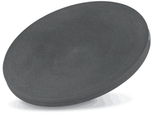
Copper sulfide is an inorganic compound with a chemical formula of CuS. It is dark brown and extremely insoluble. It is one of the most insoluble substances (second only to silver sulfide, mercury sulphide, palladium sulfide and platinous sulfide).

 Copper Sulfide Sputtering target
Copper Sulfide Sputtering target

Copper sulfide sputtering targets can be used in the semiconductor industry for the fabrication of thin film deposition from different materials for processing of integrated circuits, fabrication of architectural window glass used for energy conversation, data storage, hybrid or microelectronics, photonics  and fabrication of CDS as well as DVDs. Copper sulfide sputtering targets have different and new-fangled dimensions and product geometries.

Continue reading “What is Copper Sulfide Sputtering target?”

What is ITO (indium tin oxide) Sputtering Target?

As its name suggests, ITO sputtering target mainly contains three elements of indium, tin and oxygen. More specifically, ITO sputtering target is a black-gray ceramic semiconductor (as shown below) formed by a series of production processes after indium oxide and tin oxide powder are mixed in a certain ratio, and then sintered in a high temperature atmosphere (1600 degrees, oxygen sintering).

ITO

As one of the most widely used transparent conducting oxides, Indium tin oxide (ITO) has good electrical conductivity and optical transparency. The transmittance and resistance of ITO are controlled by the ratio of In2O3 to SnO2, respectively, and the performance is usually best when SnO2:In2O3=1:9. The most common method for preparing ITO films is physical vapor deposition (PVD). To know more information about PVD technology, please read this article What are the uses of PVD (Physical Vapor Deposition) coating. And, to know more about how to produce ITO target, please read another article Four main molding methods for ITO (Indium Tin Oxide) targets.

Continue reading “What is ITO (indium tin oxide) Sputtering Target?”

Manufacturing process of semiconductor wafer

Semiconductor wafers are the basic material for manufacturing chips. The most important raw material for semiconductor integrated circuits is silicon, which is widely found in rocks and gravel in the form of silicate or silicon dioxide in nature. The manufacturing process of semiconductor wafers/silicon wafers can be divided into three basic steps: silicon purification, monocrystalline silicon growth, and wafer formation.

Silicon purification

The sandstone material is placed in a 2000 °C electric arc furnace which has a carbon source. At high temperatures, the silica in the carbon and in the sandstone undergoes a chemical reaction (carbon is combined with oxygen, leaving silicon) to obtain pure silicon having a purity of about 98%, also known as metallurgical grade silicon. Continue reading “Manufacturing process of semiconductor wafer”

Differences between vacuum evaporation and sputter coating

It is well known that vacuum coating has two common methods: vacuum evaporation and sputter coating. However, many people have doubts about the difference between evaporation and sputter coating. Let SAM Sputter Targets answer it for you.

sputter coating3
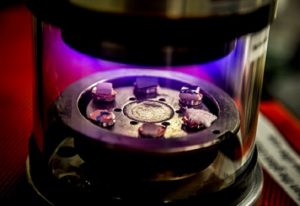
First, let’s take a look at the definition of these two words. The vacuum evaporation is carried out by means of resistance heating, electron beam or laser bombardment in an environment with a vacuum of not less than 10-2 Pa, and the evaporation material is heated to a certain temperature to evaporate or sublimate a large number of molecules or atoms, and then directly deposited on a substrate to form a film. Continue reading “Differences between vacuum evaporation and sputter coating”