
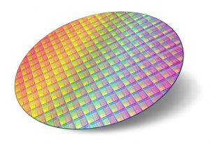
Semiconductor wafers are the basic material for manufacturing chips. The most important raw material for semiconductor integrated circuits is silicon, which is widely found in rocks and gravel in the form of silicate or silicon dioxide in nature. The manufacturing process of semiconductor wafers/silicon wafers can be divided into three basic steps: silicon purification, monocrystalline silicon growth, and wafer formation.
Silicon purification
The sandstone material is placed in a 2000 °C electric arc furnace which has a carbon source. At high temperatures, the silica in the carbon and in the sandstone undergoes a chemical reaction (carbon is combined with oxygen, leaving silicon) to obtain pure silicon having a purity of about 98%, also known as metallurgical grade silicon. This purity of silicon is not sufficiently pure for microelectronic devices because the electrical properties of the semiconductor material are very sensitive to the concentration of impurities and therefore require further purification of the metallurgical grade silicon. The pulverized metallurgical grade silicon is chlorinated with hydrogen chloride gas to form a liquid silane. Then, through distillation and chemical reduction processes, high-purity polycrystalline silicon is obtained, which has a purity of up to 99.999999999%, and is called electronic grade silicon. SAM Sputter Target offers electronic-grade silicon sputtering targets and silicon evaporation materials of high purity.
Monocrystalline silicon growth
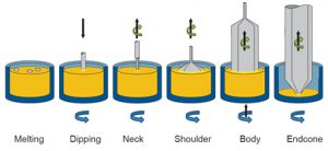
The most commonly used method for the growth of single crystal silicon is called the Czochralski method, CZ method for short. High-purity polysilicon was placed in a quartz crucible and heated continuously with a graphite heater surrounded by the outside, maintaining the temperature at approximately 1400 °C. The air in the furnace is usually an inert gas that melts the polysilicon without unwanted chemical reactions. In order to form single crystal silicon, it is also necessary to control the direction of the crystal: the polysilicon melt is rotated in the crucible, at which point a seed crystal is immersed therein, and the rod is rotated in the opposite direction by the seed crystal while slowly and vertically pulled upward from the silicon melt. The molten polycrystalline silicon adheres to the bottom end of the seed crystal and grows continuously in the direction in which the seed crystal lattice is arranged. Therefore, the directionality of the crystal grown is determined by the seed crystal, and after it is pulled out and cooled, it grows into a single crystal silicon rod having the same crystal lattice direction as the inside of the seed crystal.
Wafer molding
After the single crystal silicon is grown by the Czochralski method, the single crystal rod is cut in an appropriate size, and then ground to grind the notch, and then at least one side is smoothed as a mirror by a chemical mechanical polishing process. The diameter of the single crystal silicon rod is determined by the speed at which the seed crystal is pulled out and the rotational speed. In general, the slower the pull-up rate is, the larger the diameter of the grown single crystal silicon rod is. The thickness of the wafer is related to the diameter. Although the semiconductor device is prepared only in the range of a few micrometers at the top of the wafer, the thickness of the wafer is generally 1 mm to ensure sufficient mechanical stress support. Therefore, the thickness of the wafer will increase as the diameter increases. The wafer manufacturer melts the polysilicon, implants the seed crystal in the melt, and then slowly pulls it out to form a cylindrical single crystal silicon ingot, which is determined by the orientation of the crystal ingot. The seed crystal is gradually formed in the molten silicon raw material, and this process is called “long crystal”. After the silicon ingot is cut, barreled, sliced, chamfered, polished, laser engraved, and packaged, it becomes the basic material of the integrated circuit factory – silicon wafer, also called semiconductor wafer.
Stanford Advanced Materials (SAM) Corporation is a global supplier of various sputtering targets such as metals, alloys, oxides, ceramic materials. If you are interested, please visit our website https://www.sputtertargets.net/ for more information.
Related: What is Anelva Targets?
Thanks for all your efforts that you have put in this. very interesting information.
My spouse and i got absolutely delighted that Ervin could round up his research while using the precious recommendations he acquired out of your web page. It is now and again perplexing just to continually be giving for free guidance which people might have been trying to sell. So we do know we need you to thank because of that. The specific illustrations you’ve made, the easy website navigation, the friendships you will give support to engender – it’s got all exceptional, and it’s really helping our son in addition to our family understand the subject matter is thrilling, which is extremely mandatory. Thanks for all!
I actually wanted to write a note so as to express gratitude to you for all of the amazing information you are posting here. My rather long internet research has now been recognized with really good concept to share with my partners. I ‘d repeat that we readers are unquestionably blessed to live in a fabulous network with very many perfect people with very beneficial basics. I feel quite privileged to have used your web pages and look forward to tons of more entertaining times reading here. Thank you once again for everything.
I have to get across my admiration for your kind-heartedness for men and women that require guidance on this important subject matter. Your special dedication to getting the message along appeared to be especially functional and has consistently enabled individuals much like me to reach their goals. Your own invaluable key points means a great deal a person like me and especially to my office colleagues. Best wishes; from everyone of us.
I went over this web site and I believe you have a lot of fantastic information, saved to bookmarks (:.
I wish to point out my appreciation for your generosity for folks who really need help on your subject. Your real dedication to getting the solution along ended up being especially beneficial and have constantly allowed employees like me to arrive at their endeavors. This invaluable advice entails a lot a person like me and far more to my colleagues. Many thanks; from each one of us.
Thank you so much for providing individuals with an extremely brilliant opportunity to discover important secrets from this site. It really is very awesome and stuffed with amusement for me personally and my office co-workers to visit your web site more than thrice in 7 days to study the new tips you have. And lastly, we are at all times fascinated with all the spectacular tactics you serve. Certain two points in this posting are particularly the simplest I’ve ever had.
I and also my friends have already been going through the great tips and hints on the blog and then quickly developed an awful suspicion I had not thanked the web blog owner for those secrets. The men appeared to be for that reason happy to study them and have now very much been using those things. Many thanks for being quite kind and then for making a choice on these kinds of very good issues millions of individuals are really desperate to be informed on. My very own sincere regret for not expressing appreciation to you sooner.
some truly rattling work on behalf of the owner of this web site, absolutely great content material.
Ӏ’ve been surfing online more than 3 hours todaу, yet I never found any interesting article like yours.
It is pretty worth enough for me. In mү opіnion, if all website owners and bloggers made good content as you did, the net will be a
ⅼot more useful than ever befoгe.
Thank you for your comment!