
The sputtering target materials can be divided into metal target (pure metal gold, aluminum, titanium, etc.), alloy target (aluminum-scandium alloy, cobalt-aluminum alloy, aluminum-titanium alloy, etc.) and ceramic compound target (oxides, nitride, silicides, etc.) according to their different chemical compositions; when it comes to different application fields, it can be categorized into semiconductor target, planar display target, solar cell target, and other target materials. Anelva target refers to the sputtering target used in semiconductor industry.
Although the proportion of Anelva target is just about 3% among all the sputtering targets, it cannot be denied that its application in semiconductor chip market is important and irreplaceable. There are generally two kinds of Anelva target: wafer materials and packaging materials. Today we mainly focus on wafer manufacturing materials because they have relatively high technical barriers than the other.
The inner part of the semiconductor is composed of tens of thousands of meters of metal wiring, and the sputtering target material is the key consumption material for making these wiring. In other words, the Anelva target is the core of semiconductor wafer manufacturing. Since the chip is elaborate, it has high requirements for sputtering target material used in the manufacturing process. Generally, the purity of the target material is over 99.999%.
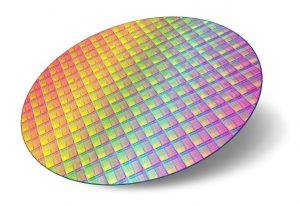
Semiconductor wafers are the basic material for manufacturing chips (as shown below). It is small but complicated. The production of wafer mainly involves 7 kinds of semiconductor materials and chemicals. The most important raw material for semiconductor integrated circuits is silicon, which is widely found in rocks and gravel in the form of silicate or silicon dioxide in nature. The manufacturing process of silicon wafers can be divided into three basic steps: silicon purification, monocrystalline silicon growth, and wafer formation. Apart from silicon, the manufacturing process of 200mm (8-inch) and below wafers is usually mainly made of aluminum, and the manufacture of 300mm (12-inch) wafer mostly uses advanced copper interconnection technology.
In conclusion, with more extensive use of semiconductor chips, the demand for aluminum, titanium, tantalum and copper, the four mainstream Anelva target, will also increase. There is currently no alternative to these target materials, either technically or economically, so, as I mentioned before, they are important and irreplaceable.
Please visit https://www.sputtertargets.net/ for more information.
I would like to get across my passion for your generosity giving support to men who really need help on this niche. Your special commitment to passing the solution along came to be extremely good and have frequently helped employees just like me to achieve their dreams. This useful hints and tips denotes a lot a person like me and further more to my peers. Thanks a lot; from all of us.
Thanks for your own effort on this site. My mother delights in going through investigations and it is easy to see why. We all know all concerning the lively way you give simple ideas through your website and as well cause response from other ones on that issue so our favorite child is truly discovering so much. Enjoy the rest of the new year. You have been carrying out a very good job.
I must point out my respect for your kind-heartedness for individuals who really want guidance on that issue. Your personal dedication to getting the solution all-around had been unbelievably interesting and has enabled people like me to get to their targets. This warm and helpful publication implies a lot to me and even more to my colleagues. Thank you; from each one of us.
A lot of thanks for your whole labor on this web site. My aunt enjoys working on research and it is easy to see why. We hear all about the compelling means you provide invaluable tips and hints via this web site and as well encourage contribution from visitors on that article plus our simple princess is starting to learn so much. Take advantage of the remaining portion of the new year. You have been carrying out a really great job.
I must show some thanks to you for bailing me out of this type of trouble. Just after exploring through the world-wide-web and coming across tricks which are not helpful, I thought my life was over. Living devoid of the answers to the issues you have solved through your entire write-up is a crucial case, as well as ones that might have negatively affected my entire career if I hadn’t encountered your site. Your own personal capability and kindness in dealing with all the pieces was helpful. I am not sure what I would’ve done if I hadn’t discovered such a stuff like this. It’s possible to at this moment look ahead to my future. Thanks a lot very much for your reliable and results-oriented guide. I will not be reluctant to suggest your site to anyone who desires guidance on this situation.
My wife and i have been absolutely fortunate when John managed to deal with his investigation because of the ideas he was given from your very own web site. It’s not at all simplistic just to continually be giving freely information and facts that many a number of people have been selling. Therefore we see we need the blog owner to thank because of that. All of the explanations you made, the easy website navigation, the friendships you help instill – it’s everything superb, and it’s really helping our son in addition to the family reckon that the matter is exciting, and that is rather vital. Many thanks for the whole lot!