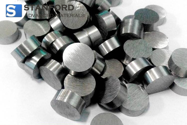
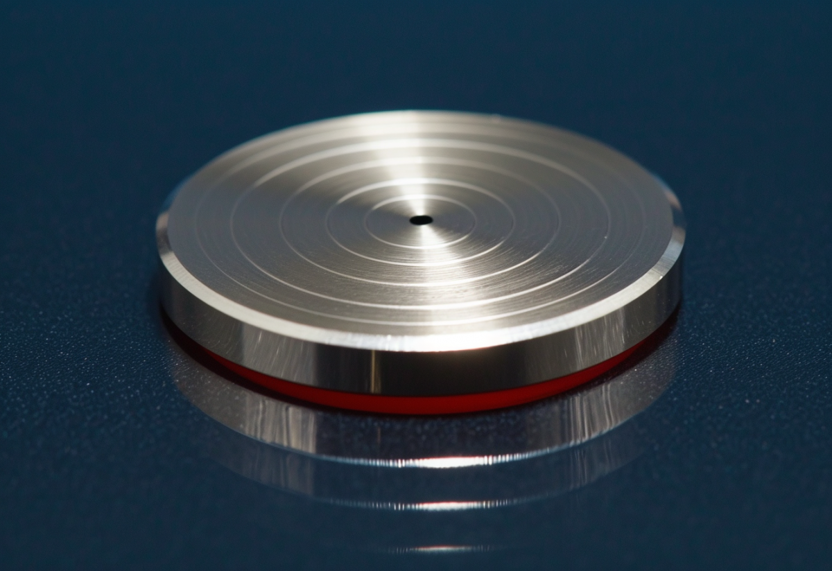
Tungsten sputtering targets are well-known for their ability to handle extremely high temperatures. Tungsten has the highest melting point of any metal at 3422°C (6192°F). This makes it one of the best materials for industries where components must work in extreme heat, such as electronics, aerospace, and semiconductors.
Key Properties of Tungsten Sputtering Targets
Tungsten’s ability to handle high temperatures is one of its greatest strengths, but it has other important features too:
High Melting Point: Tungsten’s melting point of over 3400°C allows it to stay stable in environments where other materials might fail. This makes it useful for processes involving high heat, like thermal evaporation.
Strong and Dense: Tungsten is one of the densest materials. This strengthens it, allowing it to endure the energy impacts during sputtering processes.
Low Thermal Expansion: Tungsten changes minimal in size when exposed to heat. This is important for thin-film applications where even slight changes can affect the uniformity of the coating.
Good Thermal Conductivity: Tungsten conducts heat efficiently, which helps prevent overheating during sputtering. This is important in the semiconductor industry, where keeping a steady temperature is essential.
Resistant to Oxidation: Though tungsten can oxidize at high temperatures in the presence of oxygen, it performs well in controlled environments like vacuum chambers or inert gas settings.
Applications of Tungsten Sputtering Targets
Because of these properties, tungsten sputtering targets are used in many industries. Some of their key uses include:
Semiconductors: Tungsten’s stability under high temperatures makes it important to make integrated circuits and transistors that can handle heat.
Aerospace Components: Parts used in aircraft and spacecraft face rapid temperature changes. Tungsten is used to coat parts that need to stay stable in these environments.
Electronics: Tungsten is often used in electronic devices, such as heat sinks and electrical contacts, to keep them from overheating.
Solar Panels: Tungsten is used in thin films for solar cells. Its ability to withstand high temperatures helps improve the efficiency of photovoltaic cells in solar power systems.
How Tungsten Compares to Other Sputtering Materials
The article “Top 10 Sputtering Target Materials that Can Withstand High Temperatures“ highlights tungsten as the top material for handling extreme heat. While other materials like tantalum, molybdenum, and silicon carbide also perform well at high temperatures, they do not reach tungsten’s level.
Tantalum: Tantalum can handle temperatures up to 3017°C (5463°F). It is great for applications where both heat and chemical resistance are needed. But it can’t match tungsten’s extreme heat endurance.
Molybdenum: Molybdenum has a melting point of 2623°C (4753°F) and is often used in aerospace and electronics. It performs well under heat, but it still cannot withstand the same level of temperature as tungsten.
Silicon Carbide (SiC): SiC can handle up to 2700°C (4892°F) and is often used in semiconductors and sensors. However, it lacks the extreme temperature endurance of tungsten.
Tungsten remains the best choice for the most demanding environments where the highest temperature resistance is needed.
Tungsten in the Sputtering Process
In sputtering, high-energy particles hit a target made of the desired material, like tungsten. This causes atoms from the target to be ejected and deposited onto a surface. Tungsten’s strength and heat resistance make it ideal for sputtering systems that operate under extreme conditions.
In industries where precision and heat resistance are critical, tungsten sputtering targets are the best option. Their ability to remain stable during sputtering ensures consistent and high-quality coatings.
Conclusion
Tungsten sputtering targets are the best choice for high-temperature applications due to their unmatched heat resistance and other important properties. They are widely used in semiconductors, aerospace, and electronics. As explained in the article “Top 10 Sputtering Target Materials that Can Withstand High Temperatures,” tungsten is the top performer when it comes to handling extreme heat, outshining other materials like tantalum and silicon carbide. Companies looking for high-quality sputtering materials can rely on Stanford Advanced Materials (SAM) to provide the best tungsten sputtering targets, ensuring optimal performance for all high-temperature needs.
The German research institute Fraunhofer Institute for Laser Technology has developed a groundbreaking metal part coating process called Extreme High Speed Laser Material Deposition (EHLA). This innovative technique promises to revolutionize the way metal coatings are applied, offering significant improvements in efficiency, speed, and environmental impact.
How EHLA Works
EHLA involves using a laser to create a molten pool on the surface of a component. A precise amount of metal powder is then added to this pool. Unlike traditional laser deposition processes, the powder in EHLA melts completely before it is deposited on the part’s surface. This ensures a thin, uniform coating that is both durable and resource-efficient. Remarkably, EHLA introduces approximately 90% of the material into the desired area, compared to just 50% in other methods.
Speed and Efficiency
The standout feature of EHLA is its exceptional speed. Coating processes using EHLA can be performed at speeds 100 to 250 times faster than conventional laser material deposition techniques. This rapid application rate drastically reduces processing time, making EHLA an attractive option for high-volume production environments.
Heat Sensitivity and Versatility
One of the key advantages of EHLA is its minimal heat generation during processing. This makes it ideal for coating heat-sensitive components without causing thermal damage. Additionally, EHLA is capable of tandem coating processing, which allows for the application of multiple layers or different materials in a single operation. This versatility opens up new possibilities for advanced coatings that can enhance the performance and longevity of metal parts.
Environmental Benefits
EHLA stands out for its environmental friendliness. The process eliminates the need for chromium, a chemical commonly used in traditional coating processes that is harmful to the environment. EHLA uses no hazardous chemicals, making it a safer and more sustainable option. Moreover, the coating adheres to the substrate in a material-locking manner, preventing peeling and ensuring a long-lasting bond.
Applications and Future Prospects
Researchers are excited about the potential applications of EHLA. The process is effective in protecting metal parts from corrosion and wear, extending the life cycle of products. It is compatible with various coatings, including iron, nickel, and cobalt-based alloys, making it suitable for a wide range of industrial applications.
With its impressive speed, efficiency, and environmental benefits, EHLA presents a promising future for metal coating technologies. It offers a sustainable solution that not only enhances the performance of metal parts but also reduces resource consumption and environmental impact.
About Stanford Advanced Materials
Stanford Advanced Materials (SAM) Corporation is a global supplier of various sputtering targets such as metals, alloys, oxides, and ceramic materials. If you are interested in learning more about EHLA or our range of products, please visit our website at SAM Sputter Targets for more information.
Tungsten sputtering targets are pivotal in numerous industrial and technological sectors, primarily due to tungsten’s outstanding properties such as high melting point, hardness, and electrical conductivity. These targets are used in various applications from electronics to decorative coatings, playing a crucial role in enhancing product performance and durability. Here’s a deeper look into the various applications of tungsten sputtering targets:
1. Semiconductor Manufacturing
In the semiconductor industry, the use of tungsten is essential for the creation of integrated circuits. Tungsten sputter targets are employed to deposit thin films that form part of the transistor structures in semiconductor devices. The metal’s excellent electrical conductivity and robustness against electromigration make it an ideal choice for metallization processes. This involves forming conductive barrier layers and contact points within semiconductor chips, which are critical for the device’s functionality and longevity.
2. Thin-Film Transistors in TFT-LCD Screens
Tungsten layers are crucial components in thin-film transistors (TFT) used in LCD screens. These screens rely on tungsten when high image definition, optimized contrast, and large screen formats are required. The properties of tungsten help in achieving precise control over the electronic properties of the screens, which is essential for enhancing the quality and clarity of the display.
3. Microelectronics
Beyond large-scale displays, tungsten targets find significant utility in the realm of microelectronics. They are used to create various layers in frequency filters such as surface acoustic wave (SAW) filters and bulk acoustic wave (BAW) filters. These components are vital in telecommunications and consumer electronics for managing signal frequencies and enhancing device performance.
4. Creation of Diffusion Barriers and Conductor Tracks
In microelectronic components, tungsten targets are used to deposit diffusion barriers made of tungsten-nitride. These barriers prevent the intermixing of different metals and maintain the integrity of the device’s architecture. Additionally, tungsten is used to form conductor tracks, which are essential for the electrical connectivity within the device.
5. Transparent Layers for OLED Displays
Reactively sputtered tungsten oxide layers are employed in the production of OLED displays. These transparent layers are critical for the display’s performance, contributing to the color purity and efficiency of the light-emitting components. The use of tungsten in such applications underscores its versatility and value in advanced display technologies.
6. Wear and Corrosion Resistant Coatings
Tungsten is extensively used for producing wear-resistant coatings for tools and machine components. These coatings significantly enhance the durability and lifespan of the tools, making them more efficient and resistant to harsh operational conditions. Similarly, tungsten’s chemical stability makes it suitable for corrosion-resistant coatings, which protect industrial equipment from environmental degradation.
7. Decorative Coatings
The robust and lustrous nature of tungsten also lends itself to decorative applications. Tungsten coatings are used to provide a durable and aesthetically appealing finish on various consumer products, combining functionality with style.
Conclusion
The applications of tungsten sputtering targets are diverse and critical across various industries. From enhancing the performance of electronic devices to providing durable solutions in harsh environments, tungsten continues to be an indispensable material in advanced manufacturing and technology development. Its unique properties not only facilitate innovation in current technologies but also pave the way for future advancements in material science and engineering.
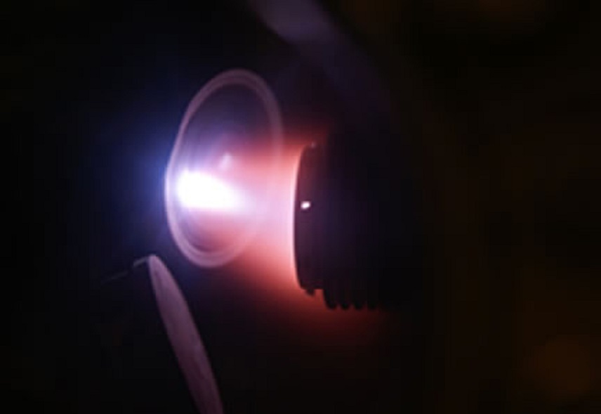
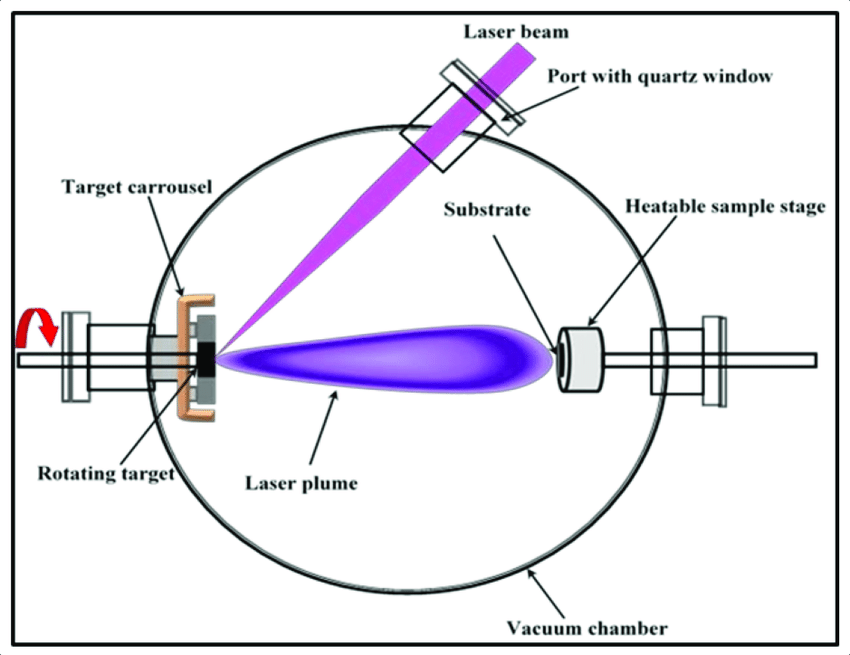
In the world of materials science, the quest for precision and versatility in thin film preparation has led to the development of several advanced techniques, among which Pulsed Laser Deposition (PLD) stands out.
PLD, also known as Pulsed Laser Ablation, harnesses the power of a laser to bombard the surface of a target material. This process elevates the surface temperature significantly, producing high-temperature and high-pressure plasma (T > 104K). The material then deposits on various substrates to form a thin film. This technique is celebrated for its ability to create films with unparalleled precision, catering to a wide range of applications from microelectronics to optical technologies.
Simplified schematic diagram illustrating the pulsed laser deposition (PLD) set-up. Ogugua, Simon & Swart, H. & Ntwaeaborwa, Odireleng. (2020). Latest Development on Pulsed Laser Deposited ThinFilms for Advanced Luminescence Applications. Coatings. 10. 1078. 10.3390/coatings10111078.
Advantages of PLD
Multi-component Films
One of the hallmark advantages of PLD is its adeptness at producing multi-component films that maintain the desired stoichiometric ratios with ease. This characteristic is particularly beneficial in applications requiring precise chemical compositions, making PLD a preferred method for developing advanced functional materials.
High Deposition Rate and Flexibility
PLD boasts a high deposition rate, ensuring a swift test period and minimal substrate temperature requirements. This efficiency, coupled with the uniformity of the films prepared, positions PLD as a highly effective method for thin film deposition. Moreover, the process’s inherent simplicity and flexibility signal its vast development potential and compatibility across a broad spectrum of materials science endeavors.
Adjustable Process Parameters
The ability to arbitrarily adjust process parameters is another feather in PLD’s cap. This flexibility allows for the easy preparation of multilayer films and heterojunctions, with no limitation on the type of PLD targets. The adaptability in choosing multi-target components further underscores PLD’s versatility in meeting diverse material preparation needs.
Non-polluting and Easy Control
Utilizing UV pulsed lasers as the energy source for plasma generation, PLD stands out as a non-polluting technique. This aspect, combined with the method’s ease of control, ensures that PLD aligns with the growing demand for environmentally friendly and easily manageable manufacturing processes in the production of thin film materials.
Disadvantages of PLD
Despite its numerous advantages, PLD is not without its challenges. One notable issue is the presence of molten small particles or target fragments in the deposited film, which can significantly compromise the quality of the film. These particles, sputtered during the laser-induced explosion, introduce defects that detract from the film’s integrity.
The feasibility of PLD for large-area deposition also remains unproven, limiting its application in industries requiring expansive film coverage. Coupled with an average deposition rate that is slow relative to other methods, these limitations suggest areas where PLD may benefit from further refinement and innovation.
Moreover, considering the cost and scale of laser film preparation equipment, PLD’s current applicability appears confined to high-tech fields such as microelectronics, sensor technology, optical technology, and new material films. This niche positioning highlights the need for continued development to expand PLD’s utility across a broader range of applications.
Stanford Advanced Materials (SAM) and PLD
In the landscape of thin film preparation, the role of reliable materials suppliers cannot be overstated. Stanford Advanced Materials (SAM) Corporation emerges as a global leader in providing a diverse array of sputtering targets, including metals, alloys, oxides, and ceramic materials. These materials are pivotal for PLD and other thin film deposition techniques, underscoring SAM’s contribution to advancing the frontiers of materials science and engineering.
Conclusion
Pulsed Laser Deposition (PLD) presents a compelling technique in the preparation of thin films, offering a unique blend of precision, versatility, and environmental friendliness. While its advantages pave the way for innovative applications, the method’s limitations highlight areas ripe for research and development. As the field continues to evolve, partnerships with materials suppliers like Stanford Advanced Materials (SAM) will be crucial in harnessing PLD’s full potential, driving forward the technological advancements that rely on high-quality thin films.
In the ever-evolving field of material science, Physical Vapor Deposition (PVD) stands as a cornerstone technology, enabling the development of high-performance coatings across a myriad of industries. At the heart of this technology lies a diverse array of materials, each selected for its unique properties to meet specific application demands. From the reflective surfaces of optical devices to the durable exteriors of aerospace components, the choice of PVD materials directly influences the functionality and efficiency of the final product. This article delves into four pivotal categories of PVD materials—sputtering targets, evaporation materials, inorganic chemicals, and specialized PVD materials—exploring their roles, properties, and the customization options that tailor them to their respective applications.
Sputtering targets play a pivotal role in the Physical Vapor Deposition (PVD) process, serving as the source material for thin film coatings. This technique involves bombarding a solid target with high-energy ions, causing atoms to be ejected and deposited onto a substrate, forming a thin film. The choice of target material, such as gold for its unparalleled electrical conductivity or chromium for its exceptional corrosion resistance, is crucial for achieving the desired properties of the final coating.
The customization of sputtering targets is a critical factor in optimizing the PVD process. By tailoring the shape, size, and composition of the target, manufacturers can ensure efficient and uniform deposition, significantly enhancing the performance of the coating. This adaptability allows for a high degree of control over the film’s thickness, composition, and microstructure, meeting the precise requirements of various applications.
Advancements in sputtering technology continue to broaden the range of applications for sputtering targets. From enhancing the durability of aerospace components to improving the efficiency of solar panels, the applications of sputtering targets are expanding into new industries. These advancements not only demonstrate the versatility of sputtering as a deposition method but also underscore the importance of continuous innovation in target material development to meet the evolving needs of technology and industry.
Evaporation Materials
In the realm of Physical Vapor Deposition (PVD), evaporation materials hold a distinct place due to their role in creating thin films through the process of material vaporization and subsequent condensation on a substrate. This method utilizes materials such as silver, known for its excellent reflective properties, making it indispensable for optical coatings. Similarly, copper, celebrated for its high thermal conductivity, is a prime choice for coatings that demand efficient heat management solutions.
The capability to customize these evaporation materials, including the development of specific alloys like Zinc Tin (Zn/Sn), enables engineers to precisely manipulate the thin film’s properties. This level of control is critical for tailoring the film’s optical characteristics, electrical conductivity, or thermal properties to suit specific application needs. By adjusting the composition, form, and purity of the evaporation material, it’s possible to achieve high-performance coatings with optimized characteristics.
Zinc Tin (Zn/Sn) Evaporation Materials
The impact of selecting the right evaporation material extends far beyond the quality of the thin film itself. It influences the efficiency of the deposition process, the durability of the coating, and ultimately, the performance of the end product. For instance, the choice of silver for reflective coatings in high-end optical applications not only enhances the product’s functionality but also its longevity. Similarly, copper’s use in thermal management coatings can significantly improve electronic devices’ performance and reliability by efficiently dissipating heat.
As PVD technologies advance, the possibilities for customizing evaporation materials expand, opening new avenues for innovation in thin-film applications. Whether it’s developing more efficient solar panels or enhancing the durability of electronic displays, the evolution of evaporation materials continues to drive the advancement of coating technologies and the industries they serve.
Inorganic Chemicals
Inorganic chemicals serve as fundamental components in the Physical Vapor Deposition (PVD) process, especially when the aim is to achieve specific optical or mechanical properties within thin films. Silicon dioxide (SiO2) and zinc sulfide (ZnS) are exemplary materials in this category, leveraged for their distinct capabilities in enhancing or manipulating light reflection and transmission, critical in optical coatings, and infrared applications, respectively.
The use of inorganic chemicals in PVD processes is highly diversified, thanks to the ability to tailor these materials to precise specifications. Silicon dioxide, for instance, is a staple in creating anti-reflective coatings, significantly reducing unwanted reflections in lenses and display screens. On the other hand, zinc sulfide finds its place in night-vision equipment, exploiting its infrared properties to enhance visibility under low light conditions.
Custom formulation of these chemicals is not uncommon in the industry. Manufacturers often require specific chemical compositions and forms, such as powders or pellets, to achieve optimal application results. This customization ensures that the PVD materials precisely match the intended application’s performance criteria, ranging from enhancing durability to improving efficiency or aesthetic qualities.
Case studies across various sectors demonstrate the effectiveness of inorganic chemicals in specialized coatings. For example, the application of silicon dioxide in the telecommunications industry has enabled the production of more efficient fiber optic cables by minimizing light loss. Similarly, the automotive sector benefits from zinc sulfide-based coatings, enhancing the durability and performance of infrared sensors used in driver-assistance systems.
These examples underscore the critical role of inorganic chemicals in advancing PVD technology and their contribution to the development of innovative products and solutions. The ability to customize these materials to meet exacting standards is a testament to the flexibility and adaptability of PVD processes, paving the way for further advancements in materials science and engineering.
Specialized PVD Materials
The category of specialized PVD materials includes advanced compounds such as silicon carbide (SiC) and aluminum nitride (AlN), each selected for its unique set of properties that address specific challenges in harsh environments and high-tech applications. These materials exemplify the innovative edge of PVD technology, offering solutions where traditional materials fall short.
Silicon Carbide (SiC) stands out for its exceptional hardness and thermal conductivity, making it an ideal candidate for protective coatings in environments subjected to extreme wear and high temperatures. Its application spans various industries, from aerospace, where engine components benefit from SiC’s durability and thermal resistance, to electronics, where SiC enhances the longevity and performance of semiconductor devices.
Silicon Carbide Powder
Aluminum Nitride (AlN), with its remarkable electrical insulation properties combined with high thermal conductivity, is particularly valuable in electronic applications. It’s used to fabricate substrates and insulating layers that can efficiently draw heat away from sensitive electronic components, thus preventing overheating and ensuring reliable operation under demanding conditions.
The role of these specialized materials in advancing PVD applications cannot be overstated. They not only provide enhanced performance and durability but also enable the development of technologies that were previously unattainable. For instance, the use of SiC in protective coatings has led to the creation of cutting tools that can operate at higher speeds and temperatures, significantly increasing productivity and reducing downtime.
Looking forward, the potential for new compounds and innovative applications of specialized PVD materials is vast. Ongoing research and development are expected to unveil materials with even greater capabilities, further expanding the horizons of what can be achieved with PVD coatings. Whether it’s developing ultra-resistant coatings for next-generation spacecraft or creating more efficient thermal management solutions for the latest electronics, specialized PVD materials are at the forefront of technological innovation.
Conclusion
The exploration of the four pivotal categories of PVD materials—sputtering targets, evaporation materials, inorganic chemicals, and specialized PVD materials—reveals the depth and breadth of options available for modern coating technologies. Each category offers unique properties that can be tailored to meet the exacting demands of various applications, from enhancing the optical performance of devices to improving the durability of components exposed to extreme conditions.
This diversity not only underscores the versatility of PVD technology but also highlights the importance of material selection in achieving the desired outcomes. Whether it’s choosing the right sputtering target for electrical conductivity or selecting a specialized material for thermal insulation, the success of PVD processes hinges on a deep understanding of material properties and their interactions with specific applications.
Looking ahead, the continued innovation and development of new PVD materials promise to further expand the capabilities of this technology. As industries push for higher performance standards and environmental sustainability, the role of advanced PVD materials will undoubtedly grow, driving new applications and improvements across a wide range of sectors.
For those navigating the complexities of PVD processes, the guidance o
experts and suppliers like Stanford Advanced Materials (SAM) can prove invaluable. SAM’s expertise in providing high-quality PVD materials, coupled with a deep understanding of industry-specific requirements, ensures that clients can make informed decisions, optimizing their processes and products for the challenges of tomorrow.
In conclusion, the role of PVD materials in advancing technological and industrial innovations cannot be overstated. As we continue to explore the potential of these materials, their impact on shaping the future of manufacturing, electronics, aerospace, and beyond is poised to be profound, marking a new era of material science and engineering excellence.
In the domain of advanced materials science, particularly in the fabrication of thin films, the unique properties of germanium sputtering targets are of paramount importance. These targets, integral to the sputtering process used in the production of semiconductor and optical devices, leverage the distinct characteristics of germanium to achieve superior performance. This article delves into the properties of germanium sputter targets, highlighting the attributes that make them essential for cutting-edge technological applications.
Semiconducting Properties of Germanium Sputter Targets
A key property that stands out is the semiconducting nature of germanium sputter targets. Germanium, with its favorable band gap, provides excellent electron mobility, which is crucial for the efficient operation of semiconductor devices. This semiconducting property is instrumental in the precise control over the electrical conductivity of thin films, a critical aspect in the manufacturing of electronic components.
Optical Qualities of Germanium Sputter Targets
The optical properties of germanium sputter targets also contribute significantly to their utility. The high refractive index and low optical dispersion of germanium make it an ideal material for infrared applications, allowing for the production of thin films that efficiently transmit infrared light. These properties are particularly beneficial for the development of infrared optics, thermal imaging systems, and other devices relying on superior optical performance.
Purity and Uniformity Achieved with Germanium Sputter Targets
The ability to achieve high levels of purity and uniformity is another hallmark of the properties of germanium sputter targets. In the sputtering process, the quality of the deposited film is heavily dependent on the purity of the target material. Germanium targets can be produced with minimal impurities, ensuring that the resulting films are of the highest quality. Uniformity in film thickness and composition is equally critical, affecting the performance and reliability of the finished product.
Thermal and Mechanical Stability of Germanium Sputter Targets
Germanium sputter targets are renowned for their thermal and mechanical stability. These properties are crucial for maintaining the integrity of the target material under the high-energy conditions of the sputtering process. The robust nature of germanium ensures that sputter targets can withstand the rigors of prolonged use, contributing to consistent film quality and extending the lifespan of the targets.
The Impact of Germanium Sputter Target Properties on Technology
The unique properties of germanium sputter targets—ranging from their semiconducting and optical characteristics to their exceptional purity, uniformity, and stability—make them invaluable in the realm of material science and thin-film technology. These properties enable the production of high-quality films that are integral to the performance of semiconductors, optical devices, and a host of other technological applications. The ability to tailor the electrical and optical properties of thin films through the precise use of germanium sputter targets opens up new possibilities for innovation across various fields.
The properties of germanium sputter targets are critical to the success of numerous advanced technological applications. By harnessing the unique semiconducting, optical, purity, uniformity, and stability properties of germanium, scientists and engineers can push the boundaries of thin-film technology, paving the way for the next generation of electronic and optical devices. As technology continues to advance, the role of germanium sputter targets and their distinctive properties will undoubtedly grow, highlighting their importance in the ongoing evolution of materials science.
In materials science and manufacturing, researchers are looking for new materials and techniques by studying rare earth metals. Ytterbium (Yb), a member of the lanthanide series, has garnered attention for its unique properties, making it a valuable candidate for sputter targets in thin-film deposition processes. This article examines the utilization of Ytterbium sputter targets in various fields that prioritize this rare metal.
Understanding Ytterbium
Ytterbium, with its atomic number 70 and symbol Yb, is a soft, malleable, and ductile metal. Its notable feature lies in its electronic configuration, particularly the partially filled 4f shell, which contributes to its intriguing magnetic and optical properties. Ytterbium exhibits a strong affinity for oxygen and can readily form oxides, making it suitable for various applications, particularly in the form of sputter targets.
Before delving into the applications, it’s essential to understand the basics of thin-film deposition techniques. Sputtering is a widely used method where energetic ions bombard a target material, causing the ejection of atoms or molecules that then form a thin film on a substrate. Ytterbium sputter targets, usually in the form of discs or rectangles, serve as the source material in this process.
Applications of Ytterbium Targets
Solar Cells and Photovoltaics:
One of the prominent applications of Ytterbium sputter targets lies in the realm of solar energy. Ytterbium-doped thin films find use in the fabrication of solar cells and photovoltaic devices. The incorporation of Ytterbium helps enhance the efficiency of solar cells by improving their light-absorbing and electron-transport properties. The versatility of Ytterbium makes it a valuable dopant for thin films, contributing to the ongoing advancements in sustainable energy technologies.
Semiconductor Industry:
Ytterbium’s unique electronic properties make it a sought-after material in the semiconductor industry. Ytterbium-doped thin films play a crucial role in the development of advanced semiconductor devices, such as field-effect transistors (FETs) and integrated circuits. The controlled deposition of Ytterbium thin films through sputtering techniques allows for precise tuning of electrical and magnetic properties, contributing to the performance enhancement of semiconductor components.
Optoelectronics and Lasers:
The optical properties of Ytterbium make it a key player in the field of optoelectronics. Ytterbium-doped thin films are utilized in the manufacturing of lasers, particularly solid-state lasers. Ytterbium-doped laser materials exhibit broad absorption bands, enabling efficient pumping and laser emission in the near-infrared region. This makes Ytterbium an ideal candidate for the development of high-performance lasers used in various applications, including materials processing and medical devices.
Magnetic Storage Devices:
The magnetic properties of Ytterbium contribute to its application in the production of magnetic storage devices. Thin films of Ytterbium are employed in the fabrication of magnetic layers in hard disk drives (HDDs) and other data storage systems. The controlled deposition of Ytterbium thin films allows for the manipulation of magnetic properties, enhancing the storage density and performance of magnetic storage media.
Medical Imaging and Radiography:
In the medical field, Ytterbium finds application in the development of contrast agents used in medical imaging techniques such as computed tomography (CT) scans. Ytterbium-based contrast agents offer improved imaging capabilities, allowing for enhanced visibility of anatomical structures. The use of Ytterbium sputter targets in the thin-film deposition process ensures the precise and controlled fabrication of these contrast agents, contributing to advancements in diagnostic imaging technologies.
Research and Development:
Ytterbium sputter targets also play a crucial role in research and development activities across various scientific disciplines. Researchers utilize Ytterbium thin films for studying the fundamental properties of materials, exploring novel electronic and magnetic phenomena, and developing cutting-edge technologies. The versatility of Ytterbium makes it an invaluable tool for scientists and engineers pushing the boundaries of knowledge and innovation.
The applications of Ytterbium sputter targets extend across a spectrum of industries, from solar energy and semiconductors to optoelectronics, data storage, medical imaging, and research. As technology continues to advance, the demand for materials with tailored properties will only intensify, reinforcing the role of rare earth metals like Ytterbium in shaping the future of materials science and advanced manufacturing. The versatility, coupled with the controllable deposition afforded by sputtering techniques, positions Ytterbium as a key player in the development of next-generation technologies across diverse fields.
Palladium Sputter Targets, with their exceptional properties and versatile nature, have become instrumental in various industries, pushing the boundaries of technological innovation. This article explores the diverse applications of Palladium Sputter Targets, shedding light on their pivotal role in shaping advancements across sectors.
1. Electronics Industry
The electronics industry stands as a prominent beneficiary of Palladium Sputter Targets. Thin films deposited using these targets play a crucial role in the production of electronic components such as capacitors and resistors. The excellent electrical conductivity of palladium ensures the reliability and performance of these components, contributing to the ever-evolving world of electronic devices.
2. Catalysis and Sensors
Palladium’s catalytic properties find applications in catalysis and sensor technologies. Palladium Sputter Targets are extensively used in catalytic converters for automobiles, where thin films of palladium facilitate the efficient conversion of harmful emissions. Additionally, palladium thin films play a vital role in sensors, including gas sensors and biosensors, owing to their sensitivity and selectivity in detecting specific substances.
3. Hydrogen Storage
The ability of palladium to absorb and release hydrogen at room temperature makes Palladium Sputter Targets indispensable in hydrogen storage applications. Thin films of palladium contribute to the development of materials that efficiently store and release hydrogen, advancing the possibilities in clean energy storage and fuel cell technologies.
4. Medical Imaging
Palladium’s exceptional X-ray absorbance properties make it a cornerstone in medical imaging applications. Palladium Sputter Targets are utilized to create thin films for X-ray detectors, enhancing the accuracy and resolution of diagnostic imaging technologies. This application is pivotal in advancing medical diagnostics, allowing for more precise and detailed imaging.
5. Fuel Cells
Palladium Sputter Targets are advantageous to the energy sector as they aid in the creation of thin films for fuel cells. These thin films boost the functionality and effectiveness of fuel cells, promoting the growth of greener and more sustainable energy solutions. The catalytic characteristics of palladium are crucial in enabling the electrochemical reactions inside fuel cells.
6. Optical Coatings
The versatile optical properties of palladium make Palladium Sputter Targets essential in the production of thin films for optical coatings. These coatings find applications in lenses, mirrors, and other optical devices, enhancing their performance and durability. The adaptability of palladium in optical applications further solidifies its role in shaping advancements in the field of optics.
7. Water Treatment
Palladium Sputter Targets have found applications in water treatment technologies. The catalytic properties of palladium enable the development of thin films that aid in the degradation of pollutants and contaminants in water, contributing to the purification and remediation of water resources.
8. Automotive Industry
Beyond catalytic converters, Palladium Sputter Targets play a role in various automotive technologies. The thin films created using these targets contribute to the development of sensors and electronic components, enhancing the overall efficiency and safety of modern vehicles.
9. Chemical Industry
In the chemical industry, Palladium Sputter Targets are employed in the creation of thin films for corrosion-resistant coatings. These coatings protect critical equipment and components from corrosion, extending their lifespan and maintaining operational integrity.
10. Biomedical Devices
Palladium Sputter Targets find applications in the development of biomedical devices. The biocompatibility of palladium thin films makes them suitable for coating medical implants and devices, ensuring compatibility with the human body and minimizing the risk of adverse reactions.
In conclusion, the applications of Palladium Sputter Targets span a vast spectrum of industries, showcasing the versatility and adaptability of this material. From electronics and catalysis to medical imaging and beyond, the unique properties of palladium contribute to technological advancements that shape our present and future. As industries continue to evolve, Palladium Sputter Targets remain at the forefront of innovation, playing a vital role in enhancing performance, efficiency, and sustainability across diverse technological landscapes.
Cobalt, a transition metal with a distinctive blue-gray appearance, has gained significant attention in various industries owing to its unique properties. One of the key applications of cobalt lies in the realm of sputter deposition, a process widely utilized in thin-film technology. Cobalt sputter targets, in particular, have emerged as crucial components in diverse applications, ranging from electronics to energy storage. In this article, we delve into the versatile applications of cobalt sputter targets and their contributions to advancing technological frontiers.
C:
Cobalt sputter targets play a pivotal role in the production of thin films for electronic devices. The sputtering process involves bombarding a target material, in this case, cobalt, with high-energy ions, causing the release of cobalt atoms. These atoms then deposit onto a substrate, creating a thin, uniform film.
In electronics, cobalt thin films are commonly used for the fabrication of magnetic layers in devices such as hard disk drives (HDDs) and magnetic sensors. The excellent magnetic properties of cobalt make it an ideal choice for ensuring the efficient operation of these electronic components.
Magnetic Recording Media:
Cobalt’s magnetic properties also find extensive application in the field of magnetic recording media. With the continuous demand for high-density data storage, cobalt sputter targets are utilized to deposit thin magnetic films on recording media, such as tapes and disks. The magnetic thin films enable the storage of vast amounts of data in a compact space, contributing to the development of advanced data storage solutions.
Energy Storage Devices:
Cobalt sputtering targets are integral to the manufacturing of electrodes for energy storage devices, particularly lithium-ion batteries. These batteries power a myriad of portable electronic devices, electric vehicles, and renewable energy systems. Cobalt thin films are employed as cathode materials due to their high energy density and stability. Researchers are actively exploring ways to optimize cobalt-based electrodes to enhance the overall performance and lifespan of lithium-ion batteries.
Photovoltaic Cells:
In the realm of renewable energy, cobalt sputter targets have found application in the production of thin films for photovoltaic cells. Thin-film solar cells are known for their flexibility and cost-effectiveness, making them suitable for various applications. Cobalt thin films contribute to the creation of efficient solar cells by facilitating the absorption and conversion of sunlight into electrical energy. As the demand for clean energy sources continues to rise, the role of cobalt in advancing solar technology becomes increasingly significant.
Wear-Resistant Coatings:
Cobalt’s exceptional hardness and wear resistance make it an ideal candidate for coatings in various industrial applications. Cobalt sputter targets are employed to deposit thin films on surfaces, enhancing their durability and resistance to wear and corrosion. This is particularly valuable in industries such as aerospace, where components exposed to harsh environments benefit from the protective qualities of cobalt coatings.
Medical Devices and Imaging:
The biomedical field also benefits from the use of cobalt sputter targets. Cobalt thin films are employed in the manufacturing of medical devices, such as sensors and implants, due to their biocompatibility and corrosion resistance. Additionally, cobalt-based thin films play a role in the development of contrast agents for magnetic resonance imaging (MRI), contributing to the accuracy and diagnostic capabilities of this medical imaging technique.
Cobalt sputter targets have become indispensable in various technological applications, spanning electronics, energy storage, renewable energy, and healthcare. The ability of cobalt to form thin, uniform films with desirable properties has paved the way for advancements in multiple industries. As technology continues to evolve, the demand for efficient and versatile materials like cobalt will likely persist, driving further innovations and applications in the world of thin-film technology.
Platinum sputter targets, integral components in diverse industries, contribute significantly to technological advancements and scientific progress. In this comprehensive exploration, we delve into the wide-ranging applications of platinum sputter targets, illuminating their pivotal role in shaping various sectors.
Semiconductor Industry:
The semiconductor industry heavily relies on platinum sputter targets for the fabrication of integrated circuits, which are the backbone of electronic devices. These targets play a crucial role in the physical vapor deposition process, facilitating the deposition of thin platinum films onto semiconductor wafers. The resulting thin films enhance the performance and miniaturization of transistors and capacitors, contributing to the relentless evolution of semiconductor technology.
Platinum’s remarkable conductivity and stability make it an ideal material for creating thin films that ensure efficient electron flow within semiconductor devices. The precision offered by platinum sputter targets is instrumental in achieving the fine details required for intricate electronic components.
Optical Coatings and Thin Films:
The optical properties of platinum, characterized by high reflectivity and low absorption, position it as a key player in optical coatings. Platinum sputter targets are employed in processes like magnetron sputtering to deposit thin films on optical surfaces. These thin films significantly enhance the reflective properties of mirrors and coatings, making them indispensable in optical devices, telescopes, and lenses.
Beyond reflectivity, platinum’s resilience allows these thin films to endure harsh environmental conditions, ensuring the longevity and sustained performance of optical components.
Biomedical Implants and Devices:
Platinum’s biocompatibility and corrosion resistance make it a preferred material in the biomedical field. Platinum sputter targets are instrumental in depositing thin films on medical implants and devices, enhancing biocompatibility, preventing corrosion, and improving overall device performance and safety.
Consider platinum-coated stents used in cardiovascular procedures, where the thin platinum film ensures compatibility with the human body, reducing the risk of adverse reactions and enhancing the device’s effectiveness.
Catalysis and Sensors:
Platinum’s catalytic prowess places it at the forefront of catalysis and sensor technologies. Platinum sputter targets play a crucial role in creating nanostructured platinum films, elevating their catalytic activity. These nanostructured films find applications in fuel cells, where they facilitate the conversion of chemical energy into electrical energy.
In the realm of sensors, platinum-thin films contribute to the development of highly sensitive and selective sensors. Gas sensors benefit from the conductivity and stability of platinum thin films, enabling precise detection of gases in diverse environments for applications in environmental monitoring, industrial safety, and healthcare.
Flexible Electronics:
The flexibility and durability of platinum sputter targets position them prominently in the realm of flexible electronics. As demand surges for flexible displays, wearable devices, and bendable electronics, platinum thin films, deposited using platinum sputter targets, play a pivotal role in creating conductive and reliable components.
Platinum’s ability to maintain electrical properties under mechanical stress renders it an ideal material for flexible electronic applications. Platinum sputter targets ensure the deposition of thin films that guarantee the longevity and robustness of flexible electronic devices.
Platinum sputter targets serve as cornerstones in research and development activities, providing a platform for exploring new materials and applications. Materials scientists and researchers leverage platinum thin films to experiment with innovative combinations and structures, pushing the boundaries of achievable feats across scientific disciplines.
Emerging technologies like quantum computing and advanced sensors often rely on platinum thin films as integral components. The precision afforded by platinum sputter targets contributes to the development of devices boasting superior electrical conductivity, magnetic properties, and resistance to environmental factors.
Environmental Considerations and Sustainable Practices:
The use of platinum sputter targets also aligns with environmental considerations and sustainable practices. Recycling platinum from used sputtering targets and electronic waste is gaining attention as a sustainable practice. Efficient recycling processes reduce the environmental impact of platinum extraction and address economic challenges associated with the scarcity of this precious metal.
Global Impact and Collaboration:
The applications of platinum sputter targets extend globally, with research and collaboration fostering advancements on an international scale. International collaboration in materials science and engineering accelerates progress in platinum-sputtering technology. Researchers from different countries contribute diverse perspectives and expertise, leading to breakthroughs that benefit a wide range of industries.
Industrial partnerships further amplify the impact of platinum sputter targets. Collaboration between research institutions and industries facilitates the development of customized platinum thin film solutions tailored to specific industrial requirements, promoting the seamless integration of this technology into various sectors.
Conclusion:
In conclusion, the applications of platinum sputter targets are extensive and influential across multiple industries. From their indispensable role in semiconductor manufacturing to their contributions to optical coatings, biomedical devices, catalysis, and flexible electronics, platinum sputter targets continue to be at the forefront of driving innovation.
The unique properties of platinum, coupled with the precision enabled by sputtering processes, make platinum sputter targets irreplaceable in creating high-quality thin films. As technology advances and new applications emerge, the versatility of platinum sputter targets ensures their sustained significance in shaping the future of various technological fields.
The evolving applications, optimization strategies, and global impact of platinum sputter targets underscore their pivotal role in the ever-expanding realm of thin-film technologies. As we look forward, the journey of platinum sputtering continues, promising further breakthroughs and transformative applications that will shape the future of multiple industries.