In the fast-paced realm of electronics, where innovation is relentless and precision is paramount, the role of silver sputtering targets is nothing short of indispensable. These unassuming components play a crucial role in the intricate process of thin film deposition, contributing to the production of electronic devices that power our modern lives.
Further Reading: Everything You Need to Know About Silver Sputter Targets
At the heart of this technology is the utilization of silver sputtering targets in physical vapor deposition (PVD) processes, a method widely employed for depositing thin films on various surfaces. The versatility of silver in these applications stems from its excellent electrical conductivity, making it a preferred choice for numerous electronic components.
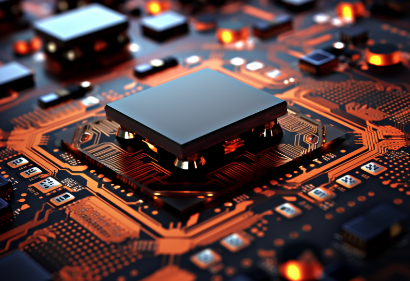
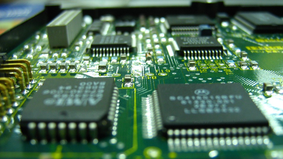
The Core of Electronic Manufacturing: Semiconductors
Semiconductors form the backbone of electronic devices, serving as the building blocks for everything from microprocessors to memory chips. Silver sputtering targets find a crucial role in the production of thin films for semiconductor devices, contributing to their functionality and performance.
In semiconductor manufacturing, precision is non-negotiable. The ability to control the thickness of the deposited film is paramount for ensuring the reliability and efficiency of electronic components. Silver sputtering targets shine in this aspect, providing manufacturers with the means to exert meticulous control over the deposition process. This precision contributes to the creation of semiconductor devices that power everything from smartphones to advanced computing systems.
Advancing Display Technologies with Silver Sputtering
The vibrant screens of televisions, computer monitors, and smartphones are a testament to the intricate layers of materials working in harmony. Silver sputtering targets play a pivotal role in the production of thin film layers for displays, enhancing the quality of visual experiences for users.
In display technologies, the demand for thin, transparent conductive films has escalated. Silver, with its exceptional conductivity, emerges as a key player in this arena. Through the sputtering process, manufacturers can precisely deposit thin layers of silver onto display surfaces, contributing to the overall performance and longevity of electronic screens.
Harnessing Solar Power with Silver Sputtering
As the world shifts towards sustainable energy sources, silver sputtering targets have found a significant application in the realm of solar cell technology. Solar cells harness the power of sunlight to generate electricity, and the efficiency of these cells is closely tied to the quality of the thin films used within them.
Silver sputtering targets contribute to the production of thin films in solar cells, improving their efficiency and enabling the conversion of sunlight into usable energy. The reflective properties of silver play a crucial role in optimizing light absorption, ultimately enhancing the overall performance of solar panels.
Enhancing Optical Surfaces: Mirrors and Beyond
The reflective glory of mirrors and the optimal performance of various optical devices owe much to the role of silver sputtering targets. In the creation of optical coatings, silver sputtering targets are employed to deposit thin films on surfaces, ensuring that mirrors and other reflective materials maintain their reflective properties.
Reflectivity is not just a matter of aesthetics but is fundamental to the functionality of optical devices like telescopes and camera lenses. By leveraging the reflective nature of silver, these devices can capture and focus light effectively, resulting in high-quality images and visual experiences.
A Silent Hero in the World of Electronics
While silver sputtering targets might not steal the spotlight in the headlines, their silent contribution is undeniably significant. From powering our electronic devices to harnessing solar energy and enhancing reflective surfaces in our daily lives, these unassuming components play a crucial role in shaping the landscape of modern technology.
The next time you marvel at the sleek design of your smartphone or enjoy the clarity of your mirror, take a moment to acknowledge the tiny silver particles working diligently behind the scenes. The remarkable process of sputtering, coupled with the unassuming silver sputter targets, exemplifies how subtle heroes contribute to the advancements and innovations that define our electronic age. As technology continues to progress, these silent heroes will likely play an even more prominent role in shaping the devices and innovations of the future.