Introduction
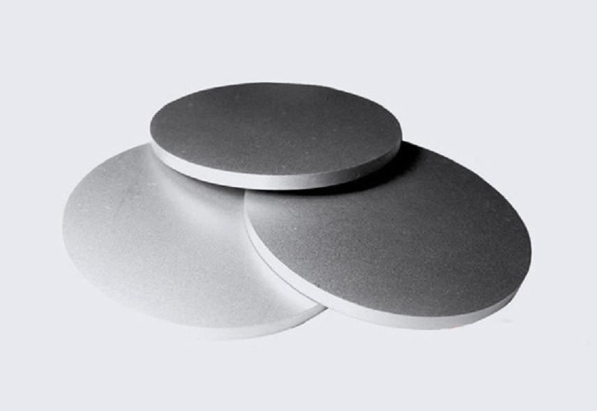
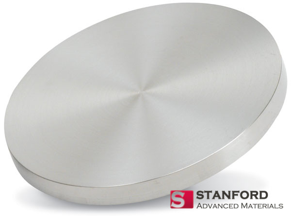
Zirconium targets are a critical component used in many different industries to create high-quality thin films through physical vapor deposition (PVD) and sputtering processes. In this article, we will explore the various benefits of zirconium targets that make them an ideal choice for researchers and manufacturers.
Consistent and Uniform Coatings
One of the primary advantages of zirconium targets is their ability to produce consistent and uniform coatings. With their excellent thermal conductivity, zirconium targets can maintain a stable temperature during the sputtering process, which helps to ensure that the resulting film is free from defects and of high quality.
Durable and Resistant to Wear
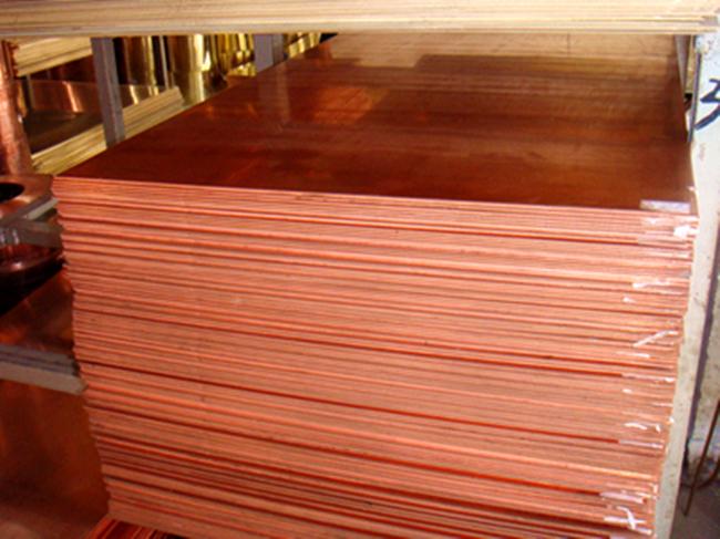
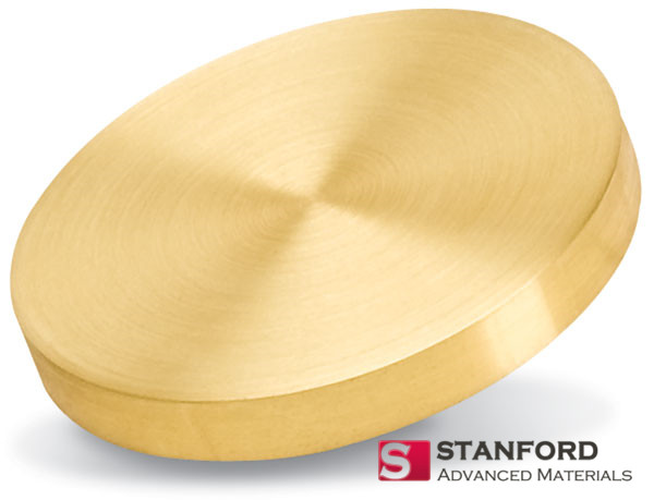
Zirconium targets are highly durable, making them an ideal choice for use in harsh or demanding operating conditions. Whether they are being used for coating medical devices, automotive parts, or aerospace components, zirconium targets are able to withstand the stresses of repeated use and exposure to harsh environments.
Versatility in Creating Complex Multilayer Coatings
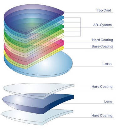
Zirconium targets are also highly versatile. Not only can they be used to create high-quality zirconium coatings, but they can also be used to deposit other materials such as aluminum, titanium, and silver. This makes zirconium targets a valuable tool for researchers and manufacturers who need to create complex multilayer coatings with precise control over the thickness and composition of each layer.
Ideal for Applications Where Purity Is Critical
Zirconium targets are an excellent choice in applications where purity is critical. Because zirconium is a highly refractory metal, it has a low affinity for impurities and can help to maintain the purity of the coating material. This is particularly important in applications such as semiconductor manufacturing, where even small amounts of impurities can have a significant impact on the performance and reliability of the final product.
Cost-Effective Solution
Finally, zirconium targets offer an attractive cost-effective option for researchers and manufacturers. Compared to other types of sputtering targets, zirconium targets are relatively low in cost, making them an accessible choice for many different applications. Additionally, their long lifespan and durability mean that they can be used for extended periods without needing to be replaced, further reducing the overall cost of operation.
Conclusion
In summary, zirconium targets are highly versatile, durable, and cost-effective, making them a valuable tool in many different industries. With their ability to produce consistent and uniform coatings, withstand harsh environments, create complex multilayer coatings, and maintain the purity, zirconium targets offer an ideal solution for meeting coating needs in a wide range of applications.
Read more on sputtertargets.net.