Can Back Target Material be Reused?

Back target materials are an essential component in the sputtering process and play a crucial role in determining the performance of thin film deposition. They serve as a support for sputtering targets, absorbing and dissipating heat generated during sputtering. It is essential to choose a suitable back target material that has good thermal conductivity, stability, and compatibility with the sputtering targets.

Furthermore, it is important to know whether the back target material can be reused or not. In this article, we will discuss the commonly used back target materials in sputtering and analyze whether they can be reused or not.

Analysis of Common Back Target Materials

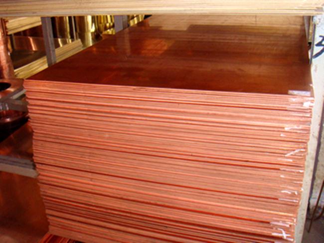
Oxygen-Free Copper (OFC)

Oxygen-free copper is the most commonly used back target material due to its good electrical and thermal conductivity. Moreover, OFC is also known for its ability to withstand high temperatures. With proper maintenance and care, an oxygen-free copper back target can be reused 10 times or more.
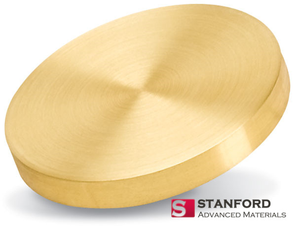
Molybdenum (Mo)

In cases where special conditions of use are required, oxygen-free copper may not serve the purpose as it can get oxidized and warped if high-temperature bonding is necessary. Therefore, molybdenum metal is used as the back target material because of its excellent thermal and electrical conductivity. Moreover, metallic molybdenum is also required as a backing material for certain ceramics and metal targets that do not have a coefficient of thermal expansion that matches oxygen-free copper.

Stainless Steel Tube (SST)

Stainless steel tubes are commonly used as a backing tube for rotating targets as they offer good strength and thermal conductivity and are very economical. They are ideal for use as a backing tube because of their resistance to corrosion and low magnetic permeability.

Can Back Target Materials be Reused?

Most back target materials can be reused, especially with metal indium for the back target, which is easier to clean and reuse compared to other materials. However, if the back target is coated with other adhesives, such as epoxy, it may be necessary to use mechanical treatment to treat the back target surface before reuse.

Conclusion

Choosing the right back target material is crucial for sputtering applications. While oxygen-free copper is the most commonly used back target material, molybdenum, and stainless steel tubes are also widely used for their unique properties.

To get high-quality sputtering targets and evaporation materials, Stanford Advanced Materials (SAM) Corporation is your best option. As a global supplier, we offer a wide range of sputtering targets such as metals, alloys, oxides, and ceramic materials, all of which have high purity. Additionally, we offer target bonding services to meet all of your needs. Visit our website at https://www.sputtertargets.net/ for more information.

Gold Sputtering Target for Semiconductor Coating

Gold sputtering targets can be deposited on a semiconductor chip such as GaAs, GaP, GaN, or the like by sputtering, and can form an ohmic contact film, an electrode, and a wiring film, thereby improving the conductivity and working efficiency of the semiconductor.

The Physical Vapor Deposition Process for Semiconductor Coatings

Physical vapor deposition (PVD) is a widely used method for depositing thin films onto semiconductor substrates such as silicon wafers. The PVD process involves the transfer of material from a sputtering target or an evaporation source to a substrate. This process is carried out in a vacuum environment to prevent contamination and ensure uniform deposition of the material.

PVD is generally divided into two methods based on the principles involved in the deposition: sputtering and evaporation.

Sputtering: How It Works and Its Variations

Sputtering is like throwing stones into a pool of mud, which will splatter a lot of mud and cover the surface of other objects. Sputtering relies on argon plasma to impact the gold sputter target at high speed, thus sputtering the material near the surface of the target and dropping it onto the wafer to form a gold film.

Sputtering is also divided into direct current (DC) sputtering and radio frequency (RF) sputtering depending on the energy source of the plasma excitation. Basically, both methods can be coated with a metal film. The latter is more directed to non-metallic films such as piezoelectric or magnetic materials. The film formed by sputtering has the characteristics of insulation and a high melting point.

Evaporation: Types and Differences from Sputtering

The evaporation method differs from the heating method and is classified into two types: a thermal coater and an E-gun evaporator. The former is to directly put the pellets prepared for melt evaporation on the heating tungsten wire. Once heated, it will adhere to the heated tungsten wire due to the surface tension of the liquid and then be steamed to the periphery (including the wafer). Due to the limited heat resistance of the heated tungsten wire and the limited space for the molten metal, it is only used for low melting point materials, and the film thickness is limited.

The electron gun-type vaporizer uses an electron beam for heating, and the molten and evaporated metal particles are all placed in a graphite or tungsten crucible. When the metal vapor pressure exceeds the critical limit, it begins to slowly evaporate for four weeks (including wafers). The electron gun-type vaporizer can evaporate a metal with a higher melting point and the thickness is not limited.

Advantages and Applications of Gold Sputtering Targets in the Semiconductor Industry

Gold sputtering targets have several advantages that make them a highly desirable material in the semiconductor industry. One of the most significant advantages of gold sputtering targets is their high electrical conductivity, making them ideal for use in forming electrodes, ohmic contacts, and wiring films in semiconductors. Furthermore, gold sputtering targets are known for their excellent adhesion properties, which ensure a strong bond to the substrate surface.

Conclusion

In conclusion, gold sputtering targets are important materials in semiconductor coating applications, and both sputtering and evaporation are commonly used methods for PVD. The choice of method depends on several factors such as deposition rate, film quality, and adherence of the deposited film required for the application. For more information, please visit https://www.sputtertargets.net/.