

Every era has some materials to follow the mainstream trend to become the leader in the industry. Under the current situation, the development of the chip industry as a high-tech commanding point has important strategic significance, and the sputter target is a necessary raw material for the manufacture of ultra-large-scale integrated circuits. Therefore, the sputtering target material may be representative of the material emerging from this mainstream trend.
In the chip industry, which is a high-tech high point, sputter targets are essential raw materials for the manufacture of very large scale integrated circuits. Very large scale integrated circuits are those with more than 100,000 components integrated on a single chip, or more than 10,000 gates. With this technology, an electronic subsystem and even the entire electronic system can be “integrated” on one chip to complete various functions such as information collection, processing, and storage. What is repeatedly used in the manufacturing process of ultra-large-scale integrated circuits is the sputtering process belonging to physical vapor deposition (PVD) technology, which is also one of the main techniques for preparing electronic thin film materials.
The principle of the sputtering process is to utilize the ions generated by the ion source to accelerate the polymerization into a high-speed ion current in a vacuum to bombard the solid surface, and the kinetic energy exchange between the ions on the surface of the ion and the solid surface causes the atoms on the solid surface to leave the target and deposit on the substrate to form a nano/micro film.
The bombarded solid is the sputtering target, which is simply like a printing mold. The quality of the target plays a crucial role in the performance of the film, which directly determines the quality and performance of downstream semiconductor chips, flat panel displays, solar cells and other electronic devices or optical components. Therefore, the sputter target is the key raw material in the whole process.
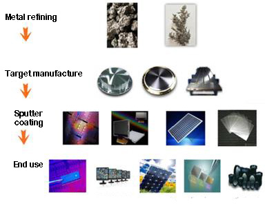
Sputtering targets can be classified according to their chemical composition, geometry and field of application. Targets with different compositions (aluminum, copper, stainless steel, titanium, nickel targets, etc.) can be divided into different film systems (superhard, wear-resistant, anti-corrosion alloy films, etc.); if divided according to their application fields, they can be divided into It is recording medium targets, semiconductor targets, display film targets, superconducting targets, and optical targets.
The target production process includes two processes of “material purification” and “target preparation”. During the purification process, it is necessary to ensure the reduction of impurity content in the target, and the preparation process needs to ensure the surface level of the sputter coater target.
Sputtering targets for high-end applications have very high technical thresholds and are very complex to prepare. First of all, it is necessary to carry out process design according to performance requirements, and then carry out repeated plastic deformation, heat treatment, precise control of grain, crystal orientation and other indicators, and then through welding, machining, cleaning and drying, vacuum packaging and other processes.
For more information, please visit https://www.sputtertargets.net/.