Introduction to Two Important Vacuum Coating Methods

In today’s electronics industry, many electronic components are manufactured using a vacuum coating process. Vacuum coating has become an indispensable technology for the manufacture of electronic components. The current vacuum coating technology is to evaporate and sputter a metal or alloy in a vacuum to deposit it on a substrate. Vacuum evaporation and magnetron sputtering coating are two main vacuum coating technologies.

Vacuum evaporation

History

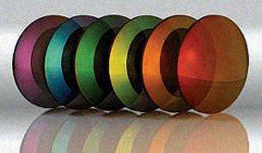
In 1857, Michael Faraday first proposed the basic principle of vacuum evaporation. Later, in the 1930s, the oil diffusion vacuum pump was put into practical use, and it was mainly used to make the lens anti-reflection film. During the Second World War, the demand for materials from other optical machines increased, and vacuum evaporation also developed rapidly.

Principle

In a vacuum state, the evaporation pellets in the evaporation vessel is heated to cause atoms or molecules to escape and deposit on the surface of the evaporation material to form a solid film. Depending on the type of vapor deposition material or substrate, it can be classified into heating methods such as resistance heating, electron beam, high-cycle induction, and laser. The vapor deposition materials include metal evaporation materials such as aluminum, lead, gold, silver, platinum, and nickel, and materials capable of producing optical properties, and oxides and fluorides such as SiO2, TiO2, ZrO2, and MgF2 are mainly used. In addition to metal, vapor deposition can be used for resin and glass, and in recent years, continuous paper has also become vapor-depositable.

Advantages

The device is simple and easy to operate; the film formation rate is fast and the efficiency is high.

Disadvantages

The thickness uniformity of the film is not easy to control, the evaporation container has hidden dangers, the process repeatability is not good, and the adhesion is not high.

Magnetron sputtering coating

History

As a very effective thin film deposition method, magnetron sputtering technology has been widely and successfully applied in many fields, especially in the fields of microelectronics, optical films and material surface treatment, for thin film deposition and surface coating preparation. In 1852, Grove first described the physical phenomenon of sputtering. In the 1940s, sputtering technology began to be applied and developed as a deposition coating method. With the rapid rise of the semiconductor industry in the 1960s, this technology was widely used and widely used in the integrated circuit production process for depositing metal electrode layers of transistors in integrated circuits. The emergence and development of magnetron sputtering technology, and the use of reflective layers for CD production in the 1980s, the field of application of magnetron sputtering technology has been greatly expanded, and gradually become a common means of manufacturing many products, and in the last ten years, a series of new sputtering techniques were developed.

Principle

Electrons accelerate to the substrate under the action of an electric field. In this process, electrons collide with argon atoms to ionize a large amount of argon ions and electrons. Under the action of an electric field, argon ions accelerate the bombardment of the sputtering target, and sputter a large number of target atoms, and the target atoms are deposited on the surface of the substrate to form a film.

Advantages

The process repeatability is good, the film has high purity, uniform film thickness and good adhesion.

Disadvantages

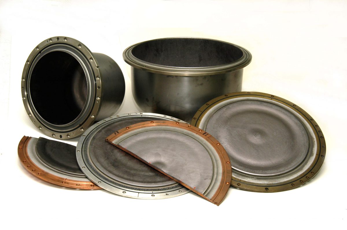
The structure of the device is complicated, and once the sputtering target penetrates, the entire target is scrapped, so the utilization rate of the target is low. Using rotatory sputtering target can increase the utilization of the target.

Please visit https://www.sputtertargets.net/ for more information.

How to Correctly Use the Sputter Coater Target (Precautions During The Sputtering Process)

Sputter coater targets have high requirements during use, requiring not only purity, size, and even grain size uniformity. These high requirements make us pay more attention when using sputtering targets. Let’s take a look at the five points of use of the sputtering coater target during use.

  1. Sputter preparation

It is very important to keep the vacuum chamber and the sputtering system clean. Any residue formed by lubricating oil and dust, as well as pre-coating, will accumulate moisture and other contaminants, directly increasing the possibility of film failure. Apart from it, the unclean sputtering chambers, sputter guns, and sputtering targets will also cause system short circuits, target arcing and rough surface formation.

In order to maintain the composition characteristics of the coating, the sputtering gas (argon or oxygen) must be cleaned and dried. After the substrate is placed in the sputtering chamber, the air needs to be extracted to achieve the vacuum level required by the process.

  1. Target cleaning

The purpose of target cleaning is the same as the first point in order to remove dust or dirt that may be present on the surface of the target and keep it clean.

  1. Target installation

The most important precaution during target installation is to ensure a good thermal connection between the target and the stabilizing wall of the sputter gun. If the warp of the cooling stave or backing plate is severe, it may cause cracking or bending of the target during installation. In this way, the thermal conductivity of the backing plate to the target is greatly affected, resulting in the inability to dissipate heat during the sputtering process, which eventually causes the target to crack or off.

  1. Short circuit and seal check

After the target is installed in the sputtering machine, it is necessary to inspect the circuit condition and seal of the cathode. It is recommended to judge whether there is a short circuit in the cathode by observing the way the resistance meter shakes. After determining that there is no short circuit in the cathode, water can be passed to the cathode to determine if there is water leakage.

  1. Target pre-sputtering

It is recommended to use pure argon for target pre-sputtering, which can help clean the surface of the target. When the sputter coating target is pre-sputtered, it is recommended to increase the sputtering power slowly. The power-increasing rate of the ceramic target is recommended to be 1.5 Wh/cm2, and the pre-sputtering speed of the metal sputter coater target materials can be 1.8 Wh/cm2 with a reasonable power increase rate compared to the ceramic target block.

For more information, please visit https://www.sputtertargets.net/.

Indium: Stable Demand in Thin Film Solar Industry

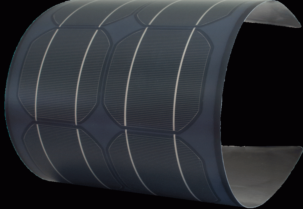
With the full arrival of the mobile energy era, the thin film solar industry grows explosively. Thin-film solar chips are light, thin, and flexible. They can be embedded in various types of carriers like Intel chips, from urban skyscrapers to neighborhood roofs, or parasols on the street, and cars running on the road. They have turned traditional products into “power generation bodies”, enabling energy sharing and free use.

Indium

Indium is one of the basic raw materials for the manufacture of thin film solar cells. Indium, atomic number 49, was discovered in 1863 by the German chemist H. Richter in zinc concentrate. Indium is silvery white and has a light blue color. The texture is very soft and can be scored with nails. In nature, indium minerals are dispersed in trace amounts in other minerals. The distribution of indium in the earth’s crust is relatively small, 1/8 of gold and 1/50 of silver. So far, no single or indium-based natural indium deposit has been found. Therefore, indium resources, in people’s impression, are scarce and difficult to mine, so that there is concern about whether there will be shortages and unstable prices of the precious metal.

Luckily, it is optimistic that the industry has said that with the improvement of mining technology, drilling technology, purification technology and recycling technology, more and more indium resources can be used. Therefore, even if the output of copper indium gallium selenide (CIGS) increases explosively in the next few years, it is difficult to affect the supply and demand of indium.

CIGS solar cell

CIGS solar cellIn the future, the copper indium gallium selenide film industry will enter a period of low-cost and high-speed development, and the thin-film solar market will be fully opened. As the photovoltaic industry continues to evolve, reducing power generation costs is a continuing goal. In this context, reducing the amount of precious indium through technical routes is a cost-reduction method that many companies are actively exploring.

At present, some companies have developed a more reliable solution to reduce the amount of indium used in copper-indium-gallium-selenide modules: developing new plasma-spray target technology, reducing the loss in sputtering target coating, reclaiming indium on residual targets, and etc. In addition, by appropriately increasing the composition of gallium or thinning the battery film layer in the copper indium gallium selenide battery, the amount of indium can also be effectively reduced.

The industry produces metal indium by purifying waste zinc and waste tin, and the recovery rate is about 60-70%. From this calculation, based on the proven reserves, the increase in recoverable amount and the indium recovery rate, the currently available indium is about 15,000 tons to 18,000 tons. If all of these indiums are used to produce copper indium gallium selenide batteries, it can produce 1,800 GW, and even if only one-tenth of the amount is used, it can produce 180 GW. In conclusion, in terms of current copper indium gallium selenide production capacity, indium resources are still very rich.

For more information about thin film coating, please visit https://www.sputtertargets.net/.


Reliable Sputtering Target Manufacturer: Stanford Advanced Materials

Part of SAM

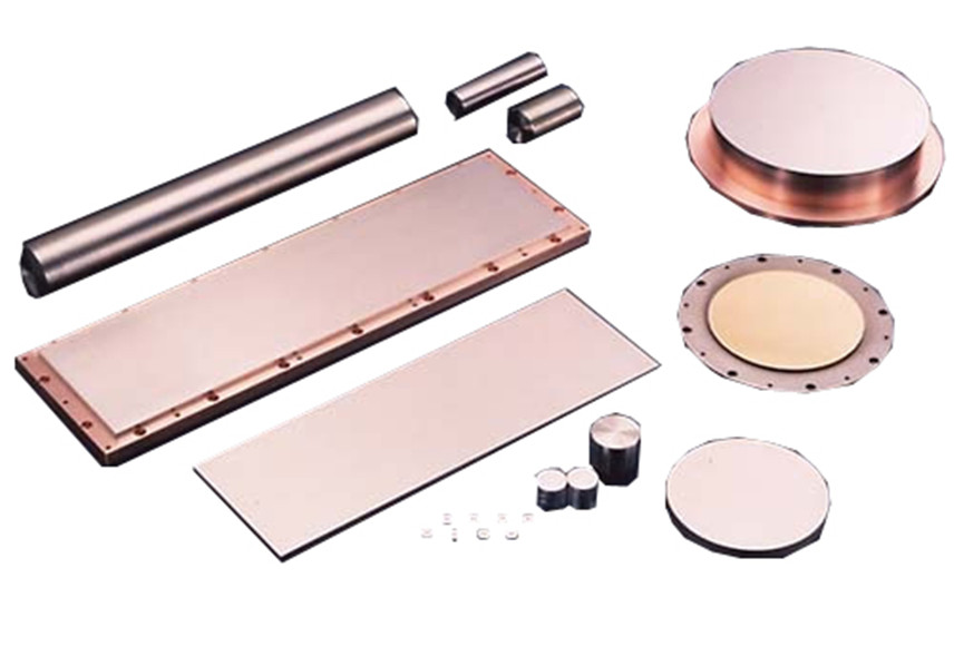
Stanford Advanced Materials (SAM) is a global supplier of a series of pure metals, alloys, ceramics and minerals such as oxides, chlorides, sulfides, oxysalts, etc. SAM Sputter Targets is a division of Stanford Advanced Materials, which specializes in manufacturing vacuum coating materials such as sputtering targets and evaporating pellets.

History of SAM

Stanford Advanced Materials was founded in 1994 and now has a history of 25 years.

SAM initially began supplying high-quality rare earth products to assist our customers in research and development (R&D). To meet the growing demand for rare earth products and other materials, SAM now offers sputtering materials not only for our R&D customers but also for manufacturers in the ceramics, metallurgical and electronics industries.

SAM supplies technology-grade materials to the industry and provides research institutions with high-purity chemicals (up to 99.99999%).

Products of SAM

SAM Sputter Targets is your reliable sputtering target manufacturer. SAM has long been committed to providing customers with high quality and reliable sputtering targets at very competitive prices.

Because we understand the importance of reliable and consistent materials to our customers’ R&D and production needs, we have established a strong relationship with our manufacturers.

By regularly visiting our manufacturers and talking to their management, production and quality control engineers and workers on the production line about the quality we seek, we have created truly effective partnerships. These valuable friendships built over the years have enabled us to deliver consistently high quality products to our global customers.

SAM’s motto is “We not only provide products, we also provide satisfactory service.” We believe that you will find SAM one of your favorite sputtering target suppliers.

What SAM Sells:

Alloy Sputtering Targets

Pure Metal Sputtering Targets

Oxide Ceramic Sputtering Targets

Planar Sputtering Targets

Rotatory Sputtering Targets

Click to see our full Product Categories.

For more information, you can contact us by email at target@samaterials.com or by calling (949) 407-8904. You can also visit our website at www.sputtertargets.net for information about our products, services, pricing and news.