Introduction
In recent years, the rapid economic development and the continuous improvement of people’s living standards have led to the continuous emergence of high-tech thin-film products, especially in the field of electronic materials and components. Vacuum coating technology has also gained significant application in this field.
At present, the common film-forming methods include vapor-phase film-forming method, oxidation method, ion implantation method, diffusion method, electroplating method, coating method, liquid-phase growth method, etc. The vapor generation method can be further subdivided into physical vapor deposition, chemical vapor deposition, and discharge polymerization.
Principle
The experiments listed in this article are related to physical vapor deposition coatings. This method is basically carried out under vacuum, so it is called vacuum coating technology.
Vacuum evaporation, sputter coating, and ion plating are commonly referred to as basic physical vapor deposition thin film preparation techniques. The vacuum evaporation coating method is a method in which the evaporation material of a film to be formed in a vaporization chamber is heated in a vacuum chamber, and atoms or molecules are vaporized from the surface to form a vapor stream, which is incident on the surface of the substrate and condensed to form a solid film.
Purposes
- To familiarize yourself with the operating procedures and methods obtained by vacuum;
- In order to understand the principle and method of evaporation coating;
- To learn how to use evaporation coating technology.
Results
(1) Vacuum conditions during evaporation
When the average free path of the vapor molecules in the vacuum vessel is greater than the distance between the evaporation source and the substrate (called the steaming distance), sufficient vacuum conditions are obtained. For this reason, it is necessary to increase the mean free path of the residual gas to reduce the collision probability of the vapor molecules with the residual gas molecules, and to evacuate the vacuum chamber to a high vacuum.
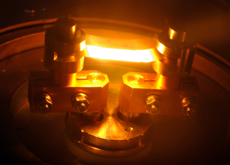
(2) How to choose evaporation source selection
1 It should have good thermal stability, chemical inactivity; the vapor pressure of the heater itself is sufficient to reach the evaporation temperature.
2 Its melting point should be higher than the evaporation temperature of the evaporated material. The heater should have a large enough heat capacity.
3 The mutual melting of the evaporated material and the evaporation source material must be very low, and it is difficult to form an alloy.
4 The material used for the coil-shaped evaporation source is required to have a good wetting with the evaporation material and a large surface tension.
5 For a case where it is difficult to form a filament, or when the surface tension of the evaporation material and the filament evaporation source is small, a boat-shaped evaporation source can be used.
(3) Main physical processes of thermal evaporation coating
1 Using various forms of thermal energy conversion to vaporize or sublimate the coating material into gaseous particles (atoms, molecules or atomic groups) with certain energy (0.1~0.3eV);
2 Gaseous particles are transported to the substrate by a substantially collision-free linear motion;
3 Particles are deposited on the surface of the substrate and agglomerated into a film.
(4) Factors affecting the quality and thickness of vacuum coating
There are many factors affecting the quality and thickness of the vacuum coating, including the degree of vacuum, the shape of the evaporation source, the position of the substrate, and the temperature of the evaporation source. The solid matter has very low evaporation at normal temperature and normal pressure. The higher the degree of vacuum, the easier it is for the molecules of the evaporation source material to scatter away from the surface of the material. The fewer molecules in the vacuum chamber, the lower the probability that the evaporating molecules will collide with the gas molecules, so that the surface of the substrate can be reached unobstructed straight.
For more information, please visit https://www.samaterials.com/.