Deformation Treatment of Aluminum Sputter Targets

Aluminum sputter targets may seem like humble components, but their journey from high-purity aluminum ingots to precision-engineered pieces involves a fascinating process known as deformation treatment. In this article, we’ll explore the intricacies of how high-purity aluminum undergoes deformation to transform into sputter targets, contributing to advancements in thin film technology.

Introduction

Aluminum sputter targets are the unsung heroes of thin film technology, and the meticulous process they undergo is crucial to their performance. The deformation treatment of aluminum, involving forging, rolling, and heating, is the key to shaping this metal into precision targets. Let’s delve into the journey of how simple aluminum evolves through a series of controlled processes to become an essential component in vacuum coating machines.

Further Reading: An Overview of Aluminum Sputter Target

High-Purity Aluminum Ingot

The journey begins with a high-purity aluminum ingot—a material of utmost importance. High purity is not just a requirement; it’s a necessity. This initial stage sets the foundation for the entire process, ensuring that the aluminum is free from impurities that could compromise the quality of the resulting sputter target.

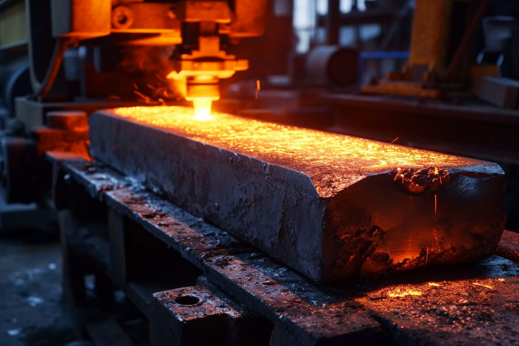
Forging: Shaping the Futur

The first significant step in the deformation treatment is forging. In simpler terms, forging involves shaping the aluminum through the application of localized compressive forces. Think of it as molding clay but on a microscopic level. The goal is to give the aluminum a preliminary form, setting the stage for subsequent processing.

forging-aluminum-ingotforging-aluminum-ingot
Forging Aluminum Ingot

Rolling: Refining the Crystal Structure

Following forging, the aluminum undergoes rolling—a process where it is passed through rollers. This isn’t just about flattening the material; it’s about refining the crystal structure. The grains in the aluminum align, creating a more uniform and controlled structure. This refinement is crucial for achieving the desired mechanical properties.

Heating: The Controlled Transformation

Heating is a crucial stage in the deformation treatment process. Controlled heating serves multiple purposes, acting as a catalyst for stress relief, recrystallization, and the elimination of any lingering imperfections. Picture it as a controlled transformation, where the aluminum undergoes changes that enhance its overall properties.

Crystal Grain Refinement and Density Enhancement

Throughout the deformation treatment, the focus is on crystal grain refinement. Finer crystal grains contribute to enhanced strength, improved conductivity, and a more uniform material. Additionally, the density of the aluminum increases, a vital aspect for ensuring the sputter target’s performance during the thin film deposition process.

Processing into Target Size

Once the deformation treatment is complete, the high-purity aluminum material is meticulously processed into the specific size and shape required for the vacuum coater. Precision machining takes center stage, ensuring that the resulting sputter target meets exact specifications, a critical factor for optimal performance.

High Precision and Surface Quality

Precision is paramount in the final stages of the deformation treatment. The processed aluminum must meet stringent standards for both high precision and surface quality. Any imperfection on the surface could compromise the performance of the sputter target, emphasizing the importance of attention to detail in this intricate process.

Conclusion

In conclusion, the deformation treatment of aluminum sputter targets is a journey that transforms a seemingly ordinary material into a crucial component of thin film technology. From the high-purity aluminum ingot to the meticulously processed sputter target, each step plays a vital role in ensuring optimal performance in vacuum coating applications.

Understanding the deformation treatment journey sheds light on the complexity behind the seemingly simple sputter targets, highlighting the precision, care, and engineering prowess required to contribute to advancements in thin film technology.

By appreciating this journey, we gain insight into how a basic metal can undergo controlled transformations, evolving into a component that drives innovation in various industries. The deformation treatment of aluminum sputter targets is a testament to the intersection of simplicity and sophistication in the world of materials science.

For more information, please visit SAM Sputter Targets.

Indium TIn Oxide in Biomedical Applications

Introduction

Indium Tin Oxide (ITO), celebrated for its prowess in transparent conducting oxides, is not confined to the realms of electronics and displays. This article delves into the fascinating intersection of ITO and biomedical applications, exploring how this versatile material is making significant contributions to the field of medicine.

ITO in Biomedical Devices: A Biocompatible Marvel

In recent years, researchers have been unlocking the potential of ITO in various biomedical applications, capitalizing on its unique blend of electrical conductivity, optical transparency, and, notably, biocompatibility. Unlike traditional materials, ITO showcases minimal inhibition of cell growth and negligible protein adsorption, making it an ideal candidate for integration into biomedical devices.

Applications in Biosensors

One notable avenue where ITO shines is in the realm of biosensors. ITO’s exceptional conductivity and transparency make it an optimal substrate for biosensor electrodes. These biosensors, equipped with ITO components, enable the precise detection of biological molecules, paving the way for advancements in medical diagnostics and disease monitoring.

ITO in Medical Imaging Devices

The marriage of ITO with medical imaging devices has yielded promising results. Its application in devices such as X-ray detectors and transparent electrodes for imaging sensors contributes to enhanced imaging quality. The superior electrical properties of ITO facilitate the creation of high-performance imaging devices crucial in medical diagnostics.

ito-in-biomedical-devices

Implantable Electronics Enhanced by ITO

The quest for more sophisticated and biocompatible implantable electronics has led researchers to ITO. As an electrode material in implantable devices, ITO offers a unique combination of electrical functionality and transparency. This is particularly valuable in devices like neural implants and bioelectronic medicine, where seamless integration with biological tissues is paramount.

ITO in Drug Delivery Systems

The controlled release of pharmaceuticals is a critical aspect of drug delivery systems. ITO’s biocompatibility and electrical properties play a role in developing smart drug delivery platforms. Researchers are exploring ITO-based systems to precisely control drug release, optimizing therapeutic outcomes and minimizing side effects.

Biomedical Advances Fueled by ITO

Enhanced Biocompatibility:

ITO’s compatibility with biological systems reduces the risk of adverse reactions, making it an attractive choice for devices directly interfacing with the human body.

Precise Bioelectronic Interfaces:

ITO’s electrical properties enable the creation of precise interfaces between electronic devices and biological tissues, fostering advancements in neuroprosthetics and bioelectronic medicine.

Real-time Monitoring and Diagnostics:

Biosensors incorporating ITO facilitate real-time monitoring of biomarkers, enabling early detection of diseases and providing valuable data for personalized medicine.

Challenges and Future Prospects

While ITO holds immense promise in biomedical applications, challenges such as long-term stability and scalability must be addressed. Researchers are actively working on innovative solutions, including advanced coatings and material enhancements, to ensure the sustained effectiveness of ITO in medical settings.

Conclusion

Indium Tin Oxide’s foray into biomedical applications is reshaping the landscape of medical technology. From biosensors to implantable electronics, ITO’s unique properties are contributing to groundbreaking innovations in diagnostics, therapeutics, and patient care. As researchers continue to unravel the potential of ITO in the realm of medicine, the collaborative synergy between materials science and healthcare promises a future where ITO plays a pivotal role in advancing biomedical technologies.

For more information, please visit https://www.sputtertargets.net/.

A Guide on Properly Handling Graphite Crucibles

Introduction:

In the realm of high-temperature applications, graphite crucibles emerge as unsung heroes, playing a crucial role in metallurgy, foundries, and laboratories. This guide is a comprehensive exploration of the proper handling of graphite crucibles, emphasizing their significance, best practices, and ways to extend their lifespan.

Understanding the Significance of Graphite Crucibles:

Graphite crucibles, crafted from high-quality graphite materials, are indispensable in processes involving extreme temperatures. Their thermal stability, resistance to chemical corrosion, and durability make them the preferred choice for applications such as metal melting, alloy production, and material analysis in laboratories.

Best Practices for Graphite Crucible Handling:

  1. Pre-Use Inspection:

    Before deploying a graphite crucible, conduct a thorough inspection. Check for any visible cracks, chips, or signs of wear. Identifying potential issues beforehand prevents crucible failure during crucial processes.

  2. Proper Installation:

    Ensure the crucible is properly installed in the furnace or melting apparatus. Improper seating can lead to uneven heating and premature wear, impacting the crucible’s performance.

  3. Temperature Gradation:

    Graphite crucibles excel in extreme temperatures, but a gradual increase in temperature is crucial. Sudden thermal shocks can lead to cracks, compromising the crucible’s integrity. Follow manufacturer guidelines for recommended heating and cooling rates.

  4. Avoiding Thermal Cycling:

    Minimize unnecessary thermal cycling, especially rapid temperature changes, as these can induce stress on the crucible material. Gradual and controlled temperature adjustments preserve the crucible’s structural integrity.

  5. Optimal Filling Levels:

    Overfilling or underfilling a crucible can impact its performance. Adhere to recommended filling levels, ensuring efficient heat transfer and preventing the risk of spillage or damage.

Extending the Lifespan of Graphite Crucibles:

  1. Regular Cleaning:

    After each use, clean the graphite crucible meticulously. Remove residual materials and contaminants to prevent cross-contamination during subsequent uses. This practice contributes to the crucible’s longevity.

  2. Protective Coatings:

    Consider applying protective coatings to the crucible’s interior surface. Coatings like boron nitride can enhance resistance to chemical reactions and minimize metal adhesion, promoting a longer crucible lifespan.

  3. Storage Conditions:

    Proper storage is essential. Keep crucibles in a dry environment to prevent moisture absorption, which can lead to internal cracks during heating.

  4. Avoiding Impact Damage:

    Handle graphite crucibles with care to prevent accidental impacts. Even minor dents or dings can compromise their structural integrity and lead to premature failure.

Troubleshooting Common Issues:

  1. Cracking:

    If a crucible develops cracks, assess their severity. Minor cracks might be manageable with proper coatings, but extensive damage may necessitate replacement.

  2. Metal Contamination:

    Metal contamination can occur due to crucible wear. Regular inspections and cleaning help identify and mitigate this issue.

Conclusion:

Mastering the art of handling graphite crucibles is pivotal in ensuring their longevity and optimal performance in high-temperature applications. From proper installation to meticulous cleaning, each step contributes to the crucible’s resilience. By adhering to these best practices, industries and laboratories can harness the full potential of graphite crucibles, ensuring precision and efficiency in their critical processes.

Further Reading: Graphite Crucibles Used for Metal Smelting

The Impact of PVD on Thin Film Transistors (TFTs)

In the dynamic landscape of semiconductor innovation, one silent hero is reshaping the very core of visual technologies – Physical Vapor Deposition (PVD). This article embarks on a journey into Thin Film Transistors (TFTs), unveiling the transformative influence of PVD techniques in their fabrication.

PVD Unveiled: The Artistry of Precision

At the heart of advanced microelectronics, PVD emerges as a masterful artisan, bringing precision and efficiency to thin film deposition processes. In the realm of TFTs, where visual brilliance meets technological intricacy, PVD’s artistry is truly unrivaled.

Enhancing TFT Performance: A Symphony of Advancements

TFTs are the backbone of modern displays, from flat-panel displays to organic light-emitting diodes (OLEDs). PVD techniques, however, elevate their performance to unprecedented levels. By depositing thin films with exceptional precision, PVD enables the creation of TFTs that redefine visual experiences.

Case in Point: High-Density Memory Storage

In the pursuit of pushing the boundaries of data storage capabilities, PVD takes center stage. Case studies abound with instances where PVD is employed to deposit thin films, enabling the creation of densely packed memory cells. The result? A maximized storage capacity coupled with enhanced data retrieval speeds, contributing significantly to the efficiency of memory devices.

Improving Response Times: The PVD Advantage

In the fast-paced world of visual content, response times are critical. PVD techniques play a pivotal role in enhancing TFT response times, ensuring a seamless and rapid transition between pixels. This not only meets the demands of today’s high-speed visual content but sets the stage for the future of display technologies.

Illustration: Performance Enhancement in Logic Circuits

Logic circuits form the neural network of semiconductor devices, and PVD’s influence extends here as well. Through controlled deposition processes, PVD ensures the creation of high-quality interconnects and metal layers, reducing resistivity and improving signal propagation. Case studies illuminate how PVD contributes to the fabrication of logic circuits with superior speed, reliability, and energy efficiency.

Reducing Power Consumption: A Green Revolution

As environmental consciousness permeates all industries, PVD takes a green stance by contributing to the reduction of power consumption in TFTs. By optimizing the materials and processes involved, PVD ensures that TFTs operate at peak efficiency with minimal energy consumption, aligning with the sustainability goals of the semiconductor industry.

Real-world Impact: Circuits in Action

The precision and reliability offered by PVD technology in TFT fabrication have a tangible impact on semiconductor memory technologies. The continual advancement of storage capacity and processing speeds is not just theoretical; it is the result of the meticulous dance of PVD on semiconductor canvases.

Further Reading: Advanced Applications of PVD in Semiconductor Devices

Conclusion: PVD’s Ongoing Symphony of Innovation

As we wrap up this exploration into the impact of PVD on TFTs, it becomes evident that PVD is not merely a technology; it is an ongoing symphony of innovation. From high-density memory storage to logic circuits and reduced power consumption, PVD’s influence is pervasive and transformative.

For those eager to delve deeper into the artistry of PVD, this article provides a glimpse into the intricate dance of precision and efficiency in TFT fabrication. The revolutionizing impact of PVD on displays is not just a trend; it is the unfolding narrative of a technology that continues to shape the future of visual experiences.

To explore more about PVD and its applications, visit SputterTargets. Join us in the ongoing symphony of innovation.