Advantage
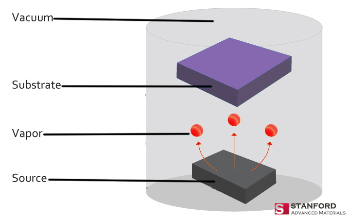
1 Ion beam sputtering relies on momentum exchange to make atoms and molecules of solid materials enter the gas phase. The average energy generated by sputtering is 10 eV, which is about 100 times higher than that of vacuum evaporation. After deposited on the surface of the substrate, these particles still have enough kinetic energy to migrate on the surface of the substrate, so that the film has good quality and is firmly bonded to the substrate.
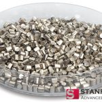
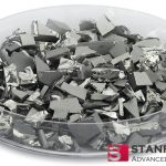
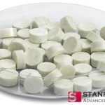
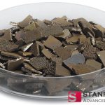
2 Any material can be coated by ion beam sputtering, and even a high-melting material can be sputtered. For alloys and compound materials, it is easy to form a film having the same ratio as the composition of the sputtering target, and thus sputter coating is widely used.
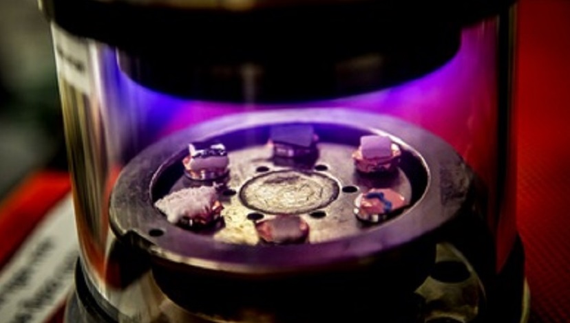
3 The incident ions of the ion beam sputter coating are generally obtained by a gas discharge method, and the working pressure is between 10-2 Pa and 10 Pa. Sputtered ions often collide with gas molecules in the vacuum chamber before flying to the substrate, so the direction of motion randomly deviates from the original direction. Sputtering is generally ejected from a larger sputter target surface area and is, therefore, more uniform than that obtained by vacuum coating. For coating parts with grooves, steps, etc., the sputter coating can reduce the difference in film thickness caused by the cathode effect to a negligible extent. However, sputtering at higher pressures will result in more gas molecules in the film.
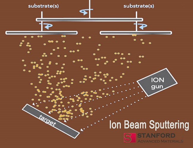
4 Sputtering can precisely focus and scan the ion beam, change the target material and substrate material while maintaining the characteristics of the ion beam, and independently control the ion beam energy and current. Since the energy of the ion beam, the beam size and the beam direction can be precisely controlled, and the sputtered atoms can directly deposit the film without collision, the ion beam sputtering method is suitable as a research method for thin film deposition.
Disadvantage
The main disadvantage of ion beam sputtering is that the target area of the bombardment is too small and the deposition rate is generally low. What’s worse, ion beam sputter deposition is also not suitable for depositing a large-area film of uniform thickness. And the sputtering device is too complicated, and the equipment operating cost is high.
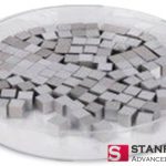
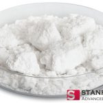
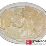
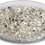
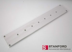
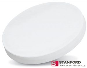
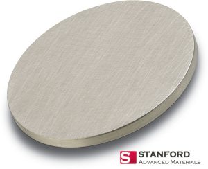
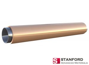
For high purity sputtering target inquiry, please visit Stanford Advanced Materials.