Introduction
Yttrium Iron Garnet (YIG) is a ferrimagnetic material distinguished by its unique properties, playing a pivotal role in advancing microwave and optical technologies. Renowned for its high Curie temperature, low damping factor, and significant magneto-optical effects, YIG is integral in developing devices requiring precise magnetic and optical performance. This article explores YIG’s magnetic and optical properties, its electrical insulating nature, crystal structure, and conductivity, underscoring its importance in modern technological applications and setting the stage for a deep dive into its versatile applications.

Comprehensive Properties of Yttrium Iron Garnet
Yttrium Iron Garnet (YIG) stands out in the materials science field for its unparalleled combination of magnetic and optical properties, underpinned by a distinctive crystal structure, alongside its capability as an electrical insulator. These attributes make YIG invaluable in a wide array of technological applications, particularly in microwave and optical devices.
Magnetic and Optical Properties
Central to YIG’s utility is its ferrimagnetic nature, distinguished by a high Curie temperature of around 560 K (287°C), allowing it to maintain magnetic properties even under elevated temperatures. This characteristic is essential for devices operating across varied thermal conditions, ensuring reliable magnetic performance. Additionally, YIG’s low damping factor minimizes energy loss during signal processing, which is critical for the efficiency of microwave electronics.
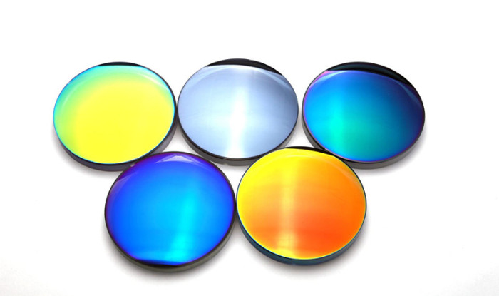
Moreover, YIG is noted for its significant magneto-optical effects, facilitating the manipulation of light based on the material’s magnetic state. This capability is exploited in the creation of optical isolators and circulators, pivotal components in optical communication systems where they enhance signal fidelity by preventing back-reflection and interference.
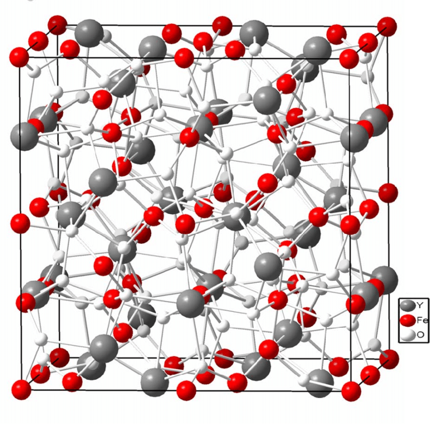
Crystal Structure and Its Influence
The remarkable properties of YIG are deeply rooted in its crystal structure. With a cubic system and garnet-type arrangement, YIG’s structure hosts yttrium, iron, and oxygen ions in a specific configuration that is key to its functionality. Yttrium ions take up dodecahedral sites, iron ions are placed in both octahedral and tetrahedral sites, and oxygen ions create tetrahedra around these metals. This precise ion distribution is instrumental in producing YIG’s ferrimagnetic behavior, facilitating the alignment of magnetic moments within the crystal lattice and contributing to its optical characteristics.
Hu, Bolin. (2015). Crystal growth of hexaferrite architecture for magnetoelectrically tunable microwave semiconductor integrated devices.
Electrical Conductivity and Insulation
Contrary to its robust magnetic and optical properties, YIG exhibits very low electrical conductivity, functioning as an electrical insulator. This trait is crucial in applications where avoiding electrical interference is necessary to maintain the integrity of the device’s operations. YIG’s insulating property ensures its compatibility in complex systems, preventing electrical currents from disrupting the desired magnetic or optical functionalities. For example, in microwave technology, the absence of electrical leakage or cross-talk due to YIG’s insulating nature is fundamental for the optimal performance of filters and oscillators.
Applications Highlighting YIG’s Unique Properties
Yttrium Iron Garnet (YIG) leverages its unique set of properties to serve a multitude of applications in the realms of microwave electronics and optical devices. Its insulating nature, coupled with exceptional magnetic and optical properties, makes it a cornerstone material for technologies that require precise control and manipulation of electromagnetic and light waves.
Microwave Electronics
In the field of microwave electronics, YIG’s ferrimagnetic properties are harnessed in the design of tunable filters and oscillators. These devices benefit from YIG’s high Curie temperature and low damping factor, which enable stable operation over a wide frequency range. The ability to fine-tune the frequency response of these components without significant loss of signal integrity is crucial for radar systems, satellite communications, and mobile telephony.
Here, YIG’s insulating nature plays a pivotal role, preventing electrical currents from interfering with the magnetic tuning processes. This ensures that the devices remain highly selective and efficient, critical factors in systems where bandwidth and signal clarity are paramount.
Optical Devices
Optical devices, particularly isolators and circulators, exploit YIG’s magneto-optical effects to control the direction and polarization of light. These components are integral to fiber optic communication networks, where signal integrity must be preserved over long distances. YIG-based optical isolators protect lasers from destabilizing feedback, while circulators direct light efficiently through the network.
The electrical insulating property of YIG is beneficial in these applications, as it eliminates the risk of crosstalk between optical and electronic components in integrated systems. This ensures that optical signals can be managed without compromise, enhancing the performance and reliability of telecommunications infrastructure.
Versatility and Importance
Beyond these applications, YIG’s versatility extends to sensors and actuators, where its sensitivity to magnetic fields enables precise measurement and control in various industrial and scientific applications. The integration of YIG in such devices underscores its importance, offering solutions that require the unique combination of its insulating, magnetic, and optical properties.
Conclusion
The exploration of Yttrium Iron Garnet (YIG) reveals a profound interconnectedness between its magnetic and optical properties, crystal structure, and insulating nature, each contributing uniquely to its versatility in advanced technological applications. From microwave electronics to optical devices, YIG’s characteristics ensure its pivotal role in enhancing the performance and reliability of contemporary technologies.
Understanding YIG not only underscores the importance of material science in driving technological innovation but also illuminates pathways for future research and development. As we delve deeper into the potential of materials like YIG, we continue to expand the horizons of what is achievable, promising exciting advancements in technology and material science.
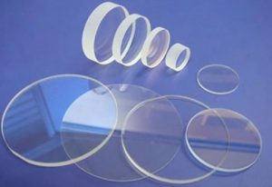
For those interested in leveraging the unique properties of Yttrium Iron Garnet (YIG) in their projects, Stanford Advanced Materials offers high-quality YIG PLD Targets and Yttrium Iron Garnet Crystal Substrates. These products exemplify the commitment to providing superior materials that meet the rigorous demands of advanced technological applications.