In the dynamic landscape of semiconductor innovation, one silent hero is reshaping the very core of visual technologies – Physical Vapor Deposition (PVD). This article embarks on a journey into Thin Film Transistors (TFTs), unveiling the transformative influence of PVD techniques in their fabrication.
PVD Unveiled: The Artistry of Precision
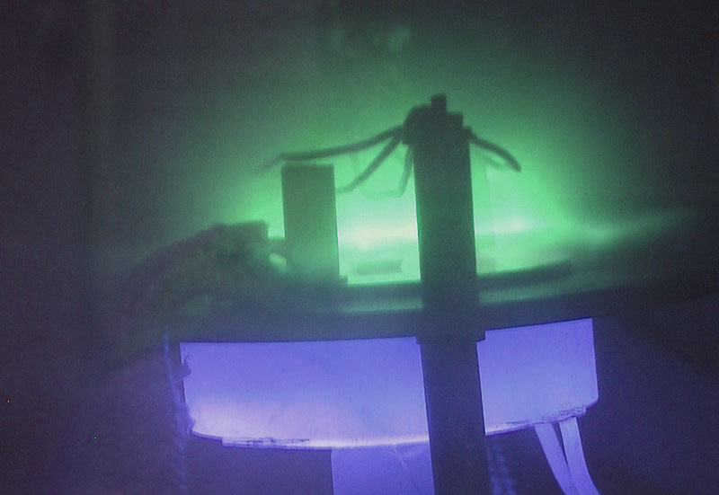
At the heart of advanced microelectronics, PVD emerges as a masterful artisan, bringing precision and efficiency to thin film deposition processes. In the realm of TFTs, where visual brilliance meets technological intricacy, PVD’s artistry is truly unrivaled.
Enhancing TFT Performance: A Symphony of Advancements
TFTs are the backbone of modern displays, from flat-panel displays to organic light-emitting diodes (OLEDs). PVD techniques, however, elevate their performance to unprecedented levels. By depositing thin films with exceptional precision, PVD enables the creation of TFTs that redefine visual experiences.
Case in Point: High-Density Memory Storage
In the pursuit of pushing the boundaries of data storage capabilities, PVD takes center stage. Case studies abound with instances where PVD is employed to deposit thin films, enabling the creation of densely packed memory cells. The result? A maximized storage capacity coupled with enhanced data retrieval speeds, contributing significantly to the efficiency of memory devices.
Improving Response Times: The PVD Advantage
In the fast-paced world of visual content, response times are critical. PVD techniques play a pivotal role in enhancing TFT response times, ensuring a seamless and rapid transition between pixels. This not only meets the demands of today’s high-speed visual content but sets the stage for the future of display technologies.
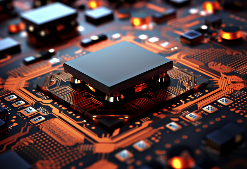
Illustration: Performance Enhancement in Logic Circuits
Logic circuits form the neural network of semiconductor devices, and PVD’s influence extends here as well. Through controlled deposition processes, PVD ensures the creation of high-quality interconnects and metal layers, reducing resistivity and improving signal propagation. Case studies illuminate how PVD contributes to the fabrication of logic circuits with superior speed, reliability, and energy efficiency.
Reducing Power Consumption: A Green Revolution
As environmental consciousness permeates all industries, PVD takes a green stance by contributing to the reduction of power consumption in TFTs. By optimizing the materials and processes involved, PVD ensures that TFTs operate at peak efficiency with minimal energy consumption, aligning with the sustainability goals of the semiconductor industry.
Real-world Impact: Circuits in Action
The precision and reliability offered by PVD technology in TFT fabrication have a tangible impact on semiconductor memory technologies. The continual advancement of storage capacity and processing speeds is not just theoretical; it is the result of the meticulous dance of PVD on semiconductor canvases.
Further Reading: Advanced Applications of PVD in Semiconductor Devices
Conclusion: PVD’s Ongoing Symphony of Innovation
As we wrap up this exploration into the impact of PVD on TFTs, it becomes evident that PVD is not merely a technology; it is an ongoing symphony of innovation. From high-density memory storage to logic circuits and reduced power consumption, PVD’s influence is pervasive and transformative.
For those eager to delve deeper into the artistry of PVD, this article provides a glimpse into the intricate dance of precision and efficiency in TFT fabrication. The revolutionizing impact of PVD on displays is not just a trend; it is the unfolding narrative of a technology that continues to shape the future of visual experiences.
To explore more about PVD and its applications, visit SputterTargets. Join us in the ongoing symphony of innovation.