As technology continues to advance, so does the need for more precise and efficient manufacturing processes. Electron beam evaporation is an important manufacturing process that uses a beam of high-energy electrons to evaporate and deposit materials onto substrates. To obtain the highest quality results, it is essential to use the correct material for the electron beam evaporation processes. Tungsten crucibles have become the go-to choice for many manufacturers due to their exceptional durability and resistance to high temperatures. In this article, we’ll explore the benefits of using tungsten crucibles for e-beam evaporation and why they have become the preferred choice for many industries. So, if you’re looking for a reliable and efficient solution for your e-beam evaporation, read on to learn more about why tungsten crucibles are the best choice.
How Tungsten Crucibles Work in E-Beam Evaporation
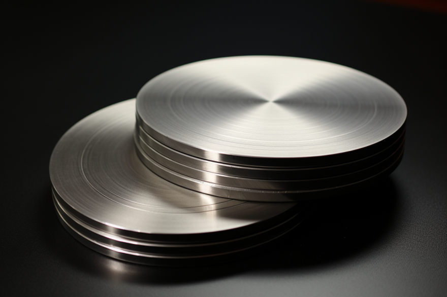
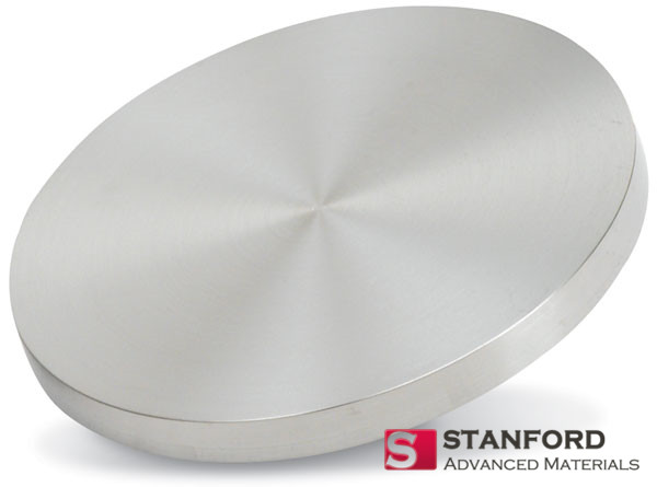
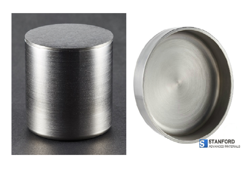
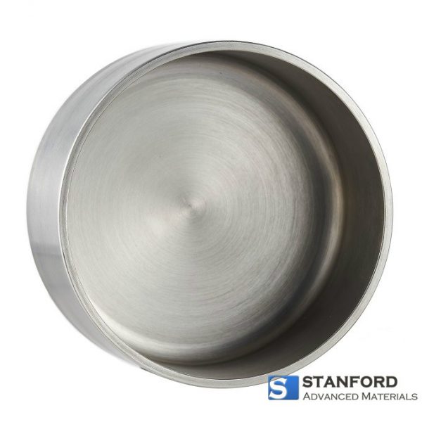
Tungsten is a metal that has a high melting point, making it ideal for use in e-beam evaporation that requires high temperatures. Tungsten crucibles are used to hold and contain the material that will be vaporized by the e-beam, such as metals or ceramics. When the e-beam is directed at the material in the crucible, it causes the material to heat up and vaporize, which is then deposited onto the substrate.
Tungsten crucibles are able to withstand the high temperatures generated by the e-beam without melting or deforming. They also have a low vapor pressure, which means that they don’t contaminate the vaporized material with tungsten particles. This is important because any contamination can affect the quality and purity of the deposited material.
Overall, the use of tungsten crucibles in e-beam evaporation allows for precise control of the vaporization process and ensures that the deposited material is of the highest quality.
Advantages of Tungsten Crucibles over Other Materials
Tungsten crucibles have several advantages over other materials that can be used in e-beam evaporation. One of the main advantages is their high melting point, which is over 3400°C. This means that they can withstand the high temperatures generated by the e-beam without melting or deforming.
Another advantage of tungsten crucibles is their low vapor pressure. This means that they don’t contaminate the vaporized material with tungsten particles, which can affect the quality and purity of the deposited material. Tungsten crucibles are also highly resistant to chemical attacks and have a long lifespan, making them a cost-effective choice for e-beam evaporation.
Tungsten Crucibles vs. Graphite Crucibles
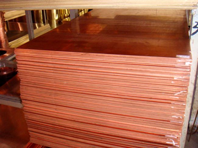
Graphite crucibles are another material that can be used in e-beam evaporation. While graphite crucibles have a lower cost than tungsten crucibles, they have several disadvantages. Graphite has a lower melting point than tungsten, which means that it can melt or deform at the high temperatures generated by the e-beam. Graphite crucibles also have a higher vapor pressure than tungsten crucibles, which can result in contamination of the vaporized material.
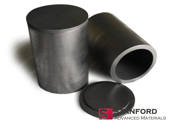
Tungsten crucibles are a better choice for e-beam evaporation than graphite crucibles due to their higher melting point, lower vapor pressure, and resistance to chemical attack.
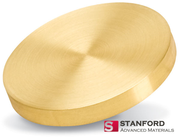
Tungsten Crucibles vs. Ceramic Crucibles
Ceramic crucibles are another alternative to tungsten crucibles for e-beam evaporation. While ceramic crucibles are less expensive than tungsten crucibles, they have several disadvantages. Ceramic crucibles have a lower melting point than tungsten, which means that they can melt or deform at the high temperatures generated by the e-beam. Ceramic crucibles are also more brittle than tungsten crucibles, which can result in cracking or breaking during use.
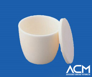
Tungsten crucibles are a better choice for e-beam evaporation than ceramic crucibles due to their higher melting point and resistance to cracking or breaking.
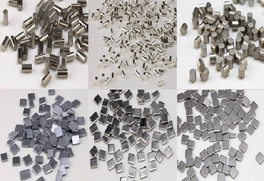
Tungsten Crucibles vs. Molybdenum Crucibles
Molybdenum crucibles are another material that can be used in e-beam evaporation. Molybdenum has a similar melting point to tungsten and is less expensive than tungsten. However, molybdenum has a higher vapor pressure than tungsten, which can result in contamination of the vaporized material.
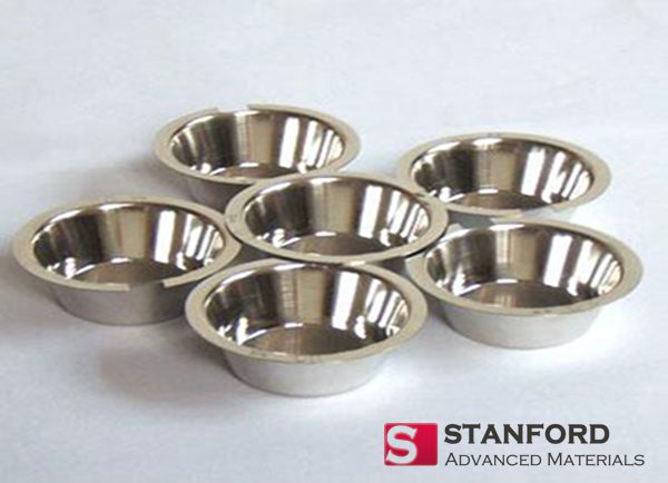
Tungsten crucibles are a better choice for e-beam evaporation than molybdenum crucibles due to their lower vapor pressure and resistance to chemical attacks.
How to Choose the Right Tungsten Crucible for Your Project
When choosing a tungsten crucible for your e-beam evaporation, there are several factors to consider. The first factor is the size of the crucible, which should be chosen based on the size of the substrate being used. The second factor is the shape of the crucible, which should be chosen based on the geometry of the substrate being used.
The third factor to consider is the thickness of the crucible. Thicker crucibles are more durable and have a longer lifespan, but they also have a higher thermal mass, which can affect the heating and cooling rates of the crucible. Thinner crucibles have a lower thermal mass, which allows for faster heating and cooling rates, but they are also less durable and have a shorter lifespan.
Overall, the choice of tungsten crucible will depend on the specific requirements of your e-beam evaporation and the materials being used.
Maintenance and Care of Tungsten Crucibles
To ensure the longevity and performance of your tungsten crucibles, it’s important to take proper care of them. Tungsten crucibles should be cleaned regularly to remove any contaminants that may affect the quality and purity of the deposited material. They should also be handled carefully to avoid any damage or cracking.
Tungsten crucibles should be stored in a dry and cool environment to prevent any corrosion or oxidation. If a tungsten crucible becomes damaged or cracked, it should be replaced immediately to avoid any contamination of the deposited material.
Conclusion: Why Tungsten Crucibles are the Best Choice for E-Beam Evaporation
Tungsten crucibles have become the go-to choice for many manufacturers due to their exceptional durability and resistance to high temperatures. They offer several advantages over other materials that can be used in e-beam evaporation, including a high melting point, low vapor pressure, and resistance to chemical attack.
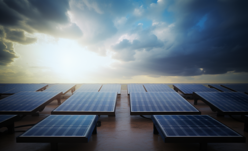
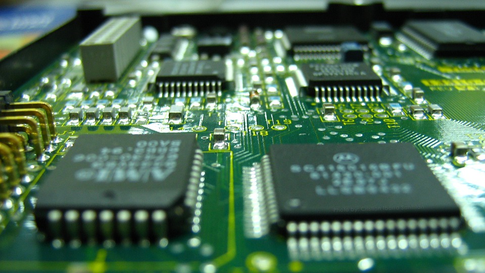
While other materials, such as graphite, ceramic, and molybdenum, may be less expensive than tungsten, they have several disadvantages that make tungsten crucibles a better choice for e-beam evaporation. Tungsten crucibles are commonly used in the semiconductor industry for the production of semiconductors, solar cells, and other electronic devices.
When choosing a tungsten crucible for your e-beam evaporation, it’s important to consider factors such as size, shape, and thickness. Proper maintenance and care of tungsten crucibles are also essential to ensure their longevity and performance.
In conclusion, if you’re looking for a reliable and efficient solution for your e-beam evaporation, tungsten crucibles are the best choice. They offer the highest quality results and are a cost-effective option for manufacturers in a variety of industries.
For more information about e-beam evaporation crucibles and related evaporation materials or sources, please visit https://www.sputtertargets.net/.