In recent years, the requirements for processing technology in various industries have been continuously improved. ITO (indium tin oxide) materials, for instance, have stricter criteria for line width and processing interval for ITO conductive patterns. The subject of whether the ITO laser etching machine can produce lines smaller than 20 microns comes up frequently. Is a 20-micron processing interval possible? The answer is yes. So what is the smallest line width of the ITO laser etching machine? Let SAM Sputter Target answer it for you.
What Determines the Line Width?
The laser and the optics define the thickness of the ITO line width, which is related to the size of the focus spot and the thermal impact of the source on the material. A line with a thinner width might be produced by a shorter wavelength because it has lower energy, a narrower pulse width, a higher beam expander magnification, a smaller field lens negative, and a smaller spot size. Several of the aforementioned parameters, of course, have a relative limit value. For instance, if the beam expander’s magnification is too great, the energy density will be inadequate and unsuitable for processing. As a result, we must choose a variety of values and apply them to the processing requirements.
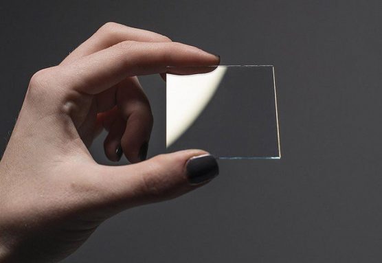
In addition, even with the same laser etch machine, the line widths made by different materials are different. For example, the etch line width of a nickel alloy material is thicker than that of an ITO material, depending on the absorption of the laser wavelength by the material itself. This article analyzes based on ITO conductive glass.
Thickness Requirements of Different Industries
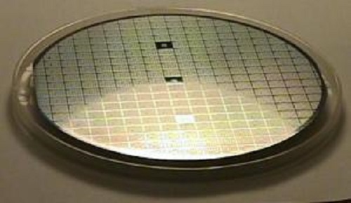
The general requirement for ITO glass in the touch screen industry is less than 20 microns, which uses a narrow pulse-width infrared nanosecond laser. Different industries have different requirements for ITO line width. In some industries, the resistance of ITO line width has relatively high requirements, while in some industries, it is required to ensure that it is cut and insulated. In the current laser market, the minimum line width of ITO conductive glass is 5 micrometers, and different line widths can be selectively selected according to different light sources. For example, the minimum line width of an ultraviolet nanosecond laser can be 15 micrometers. Of course, there are also EUV lithography machines that can achieve nanometer levels by means of extreme ultraviolet lasers. The requirements for line width are mainly determined by different product requirements.
Thinner is Better?
From the above, you can see that different industries have different thickness requirements for ITO glass. What is certain is that the thinner is not always the better. It still needs to be designed and manufactured according to the specific application.