At present, reactive sputtering deposition is a well-established sputter coating technology and is widely used for industrial coating deposition to produce thin layers for high-added value products, such as flat panel displays, solar cells, optical components, and decorative finishes.
Definition
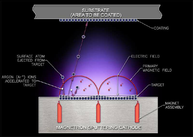
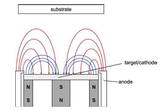
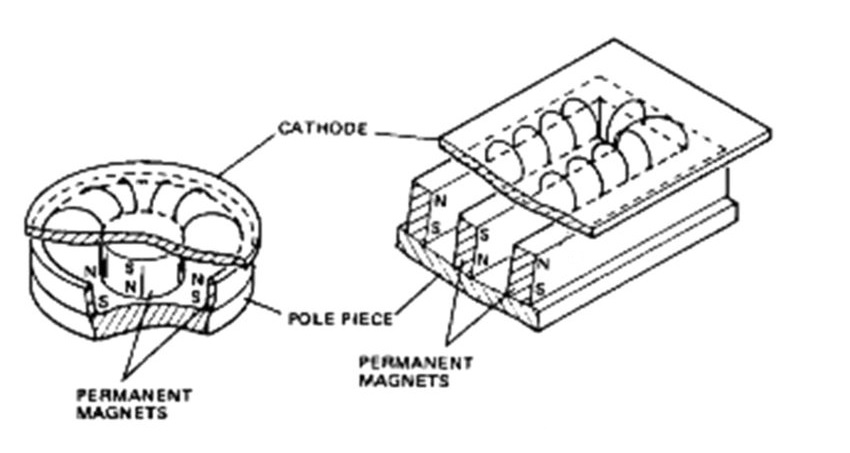
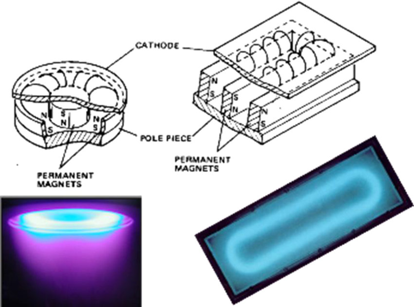
In the process of reactive sputtering, a target material is sputtered in the presence of a gas or a mixture of gasses that will react with the target material to prepare a compound film of a predetermined chemical ratio. Reactive sputtering is most often practiced using one or more magnetron sputtering cathodes. Therefore, it is also called reactive magnetron sputtering.
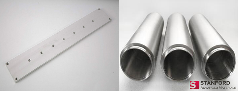
Sputtering Target
Sputtering targets can be divided into metal targets, alloy targets, ceramic targets, etc. Metal sputtering targets can be used to produce compound materials. For example, a titanium sputtering target can be used to produce coatings such as TiO2, TiN, and Ti-O-N. Apart from it, titanium targets can also be used to produce any of the aforementioned different compositions as well as boride and carbide films. Compared with the compound target, the metal target has the advantage of longer service life.
Reactive gases
In most cases, Argon is the main gas used in reactive sputtering as well as other sputter coating methods. It has to be mentioned that the amount of a reactive gas introduced into a process chamber should be strictly controlled in order to either achieve a certain amount of doping or to produce a fully reacted compound. Here is a list of other gasses used in reactive sputtering).
| Gasses | Uses |
| Oxygen (O2) | deposition of oxide films (e.g. Al2O3, SiO2, TiO2, HfO2, ZrO2, Nb2O5, AZO, ITO) |
| Nitrogen (N2) | deposition of nitride films (e.g. TiN, ZrN, CrN, AlN, Si3N4, AlCrN, TiAlN) |
| Carbon dioxide (CO2) | deposition of oxide coatings |
| Acetylene (C2H2) | deposition of metal-DLC, hydrogenated carbide, carbo-nitride films |
| Methane (CH4) | similar applications as for C2H2 |
Several reactive gasses can be mixed in order to deposit a multi-component functional thin film. Additional reactive gas is sometimes used to enhance a certain deposition process (e.g. addition of N2 in the SiO2 reactive sputtering process).

Application
Coatings and films produced by Reactive Magnetron Sputtering can be used in a large variety of products such as OLED devices, optical antireflective coatings, and decorative coatings.
Please visit https://www.sputtertargets.net/ for information.