Introduction
In materials science and manufacturing, researchers are looking for new materials and techniques by studying rare earth metals. Ytterbium (Yb), a member of the lanthanide series, has garnered attention for its unique properties, making it a valuable candidate for sputter targets in thin-film deposition processes. This article examines the utilization of Ytterbium sputter targets in various fields that prioritize this rare metal.
Understanding Ytterbium
Ytterbium, with its atomic number 70 and symbol Yb, is a soft, malleable, and ductile metal. Its notable feature lies in its electronic configuration, particularly the partially filled 4f shell, which contributes to its intriguing magnetic and optical properties. Ytterbium exhibits a strong affinity for oxygen and can readily form oxides, making it suitable for various applications, particularly in the form of sputter targets.
Read more: Ytterbium: Rare Earth Element and Application
Thin-Film Deposition Techniques
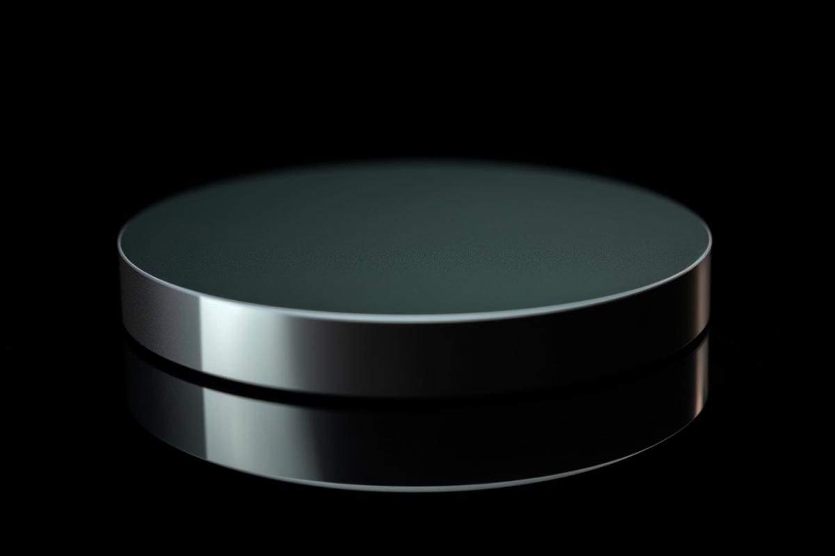
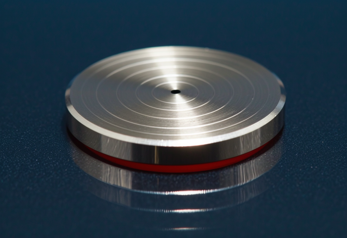
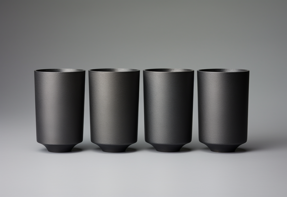
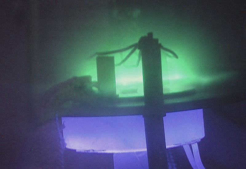
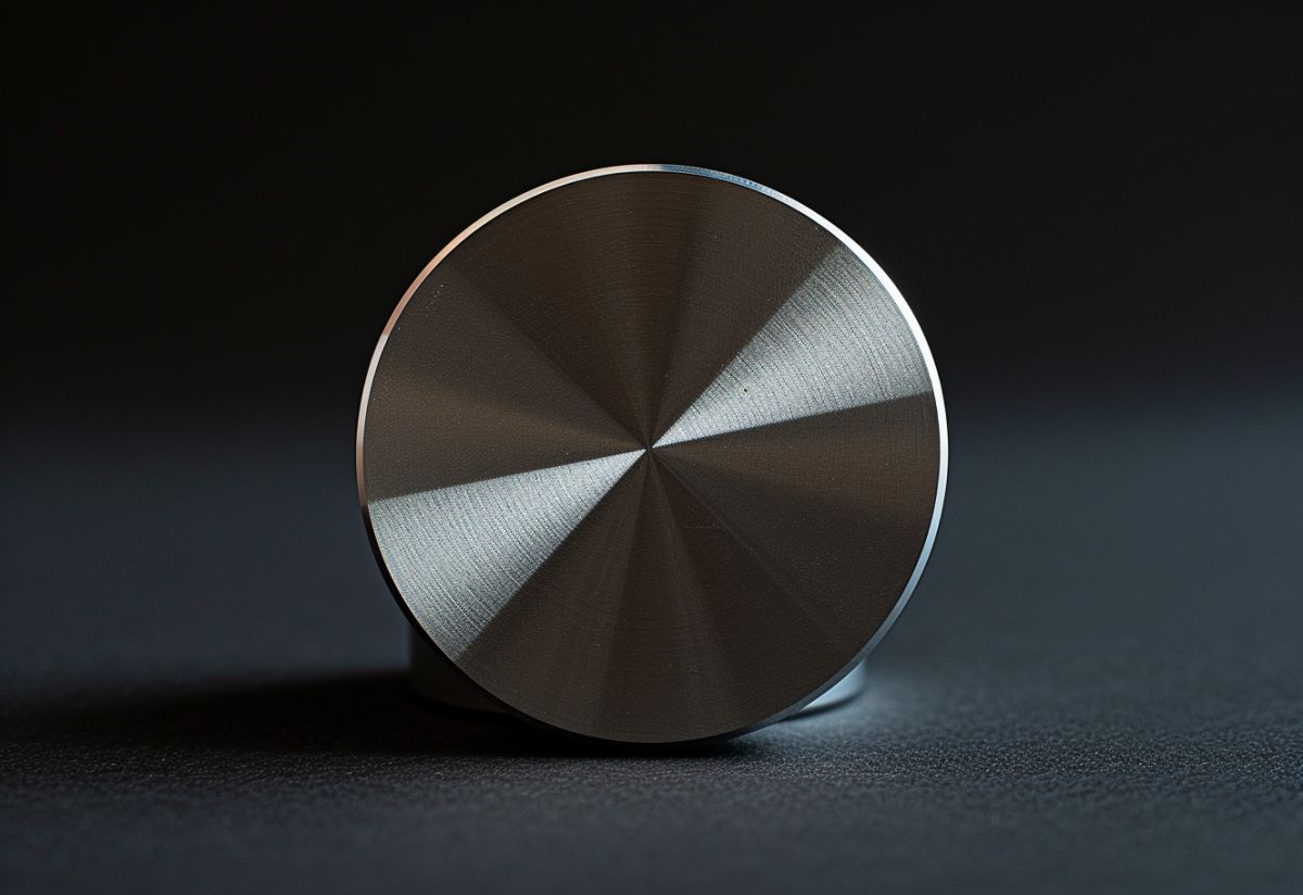
Before delving into the applications, it’s essential to understand the basics of thin-film deposition techniques. Sputtering is a widely used method where energetic ions bombard a target material, causing the ejection of atoms or molecules that then form a thin film on a substrate. Ytterbium sputter targets, usually in the form of discs or rectangles, serve as the source material in this process.
Applications of Ytterbium Targets
Solar Cells and Photovoltaics:
One of the prominent applications of Ytterbium sputter targets lies in the realm of solar energy. Ytterbium-doped thin films find use in the fabrication of solar cells and photovoltaic devices. The incorporation of Ytterbium helps enhance the efficiency of solar cells by improving their light-absorbing and electron-transport properties. The versatility of Ytterbium makes it a valuable dopant for thin films, contributing to the ongoing advancements in sustainable energy technologies.
Semiconductor Industry:
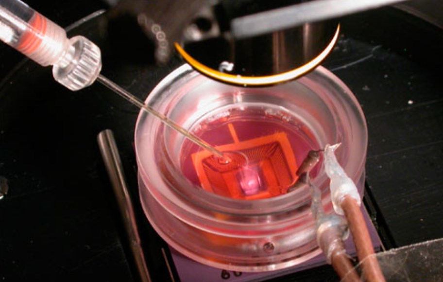
Ytterbium’s unique electronic properties make it a sought-after material in the semiconductor industry. Ytterbium-doped thin films play a crucial role in the development of advanced semiconductor devices, such as field-effect transistors (FETs) and integrated circuits. The controlled deposition of Ytterbium thin films through sputtering techniques allows for precise tuning of electrical and magnetic properties, contributing to the performance enhancement of semiconductor components.
Optoelectronics and Lasers:
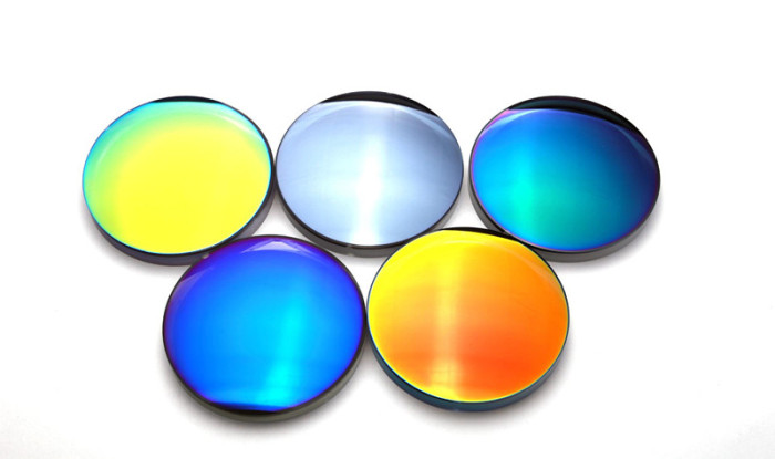
The optical properties of Ytterbium make it a key player in the field of optoelectronics. Ytterbium-doped thin films are utilized in the manufacturing of lasers, particularly solid-state lasers. Ytterbium-doped laser materials exhibit broad absorption bands, enabling efficient pumping and laser emission in the near-infrared region. This makes Ytterbium an ideal candidate for the development of high-performance lasers used in various applications, including materials processing and medical devices.
Magnetic Storage Devices:
The magnetic properties of Ytterbium contribute to its application in the production of magnetic storage devices. Thin films of Ytterbium are employed in the fabrication of magnetic layers in hard disk drives (HDDs) and other data storage systems. The controlled deposition of Ytterbium thin films allows for the manipulation of magnetic properties, enhancing the storage density and performance of magnetic storage media.
Medical Imaging and Radiography:
In the medical field, Ytterbium finds application in the development of contrast agents used in medical imaging techniques such as computed tomography (CT) scans. Ytterbium-based contrast agents offer improved imaging capabilities, allowing for enhanced visibility of anatomical structures. The use of Ytterbium sputter targets in the thin-film deposition process ensures the precise and controlled fabrication of these contrast agents, contributing to advancements in diagnostic imaging technologies.
Research and Development:
Ytterbium sputter targets also play a crucial role in research and development activities across various scientific disciplines. Researchers utilize Ytterbium thin films for studying the fundamental properties of materials, exploring novel electronic and magnetic phenomena, and developing cutting-edge technologies. The versatility of Ytterbium makes it an invaluable tool for scientists and engineers pushing the boundaries of knowledge and innovation.
Read more: Everything You Need to Know About Ytterbium Sputter Target
Conclusion
The applications of Ytterbium sputter targets extend across a spectrum of industries, from solar energy and semiconductors to optoelectronics, data storage, medical imaging, and research. As technology continues to advance, the demand for materials with tailored properties will only intensify, reinforcing the role of rare earth metals like Ytterbium in shaping the future of materials science and advanced manufacturing. The versatility, coupled with the controllable deposition afforded by sputtering techniques, positions Ytterbium as a key player in the development of next-generation technologies across diverse fields.