Advantages of Investing in Platinum and Palladium Precious Metals

Platinum and palladium are in the class of precious metals just like gold and silver in spite of little information concerning their investments. The difference is that they are not in form of currency because they are in form of industrial metal, and belong to a group called platinum metals group.

Platinum
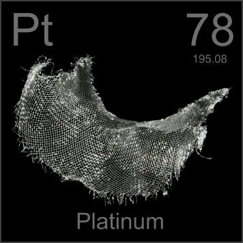
The fact that platinum is not a monetary metal confers advantages and disadvantages alike. First, it can be affected by demand issues due to its industrial nature and hence suffer massive price fluctuations sue to speculation. Secondly, it does not have the global attraction that gold and silver have as monetary metals. However, the fact that it non-monetary ensures that it is not targeted for confiscation as is the case with silver and gold. Second, the historic hart of the metal has shown that its price goes hand in hand with gold value over time even though it is more of an industrial metal. This tells you that it is a worth investment.

Related: Platinum Sputtering Target

Ways to Buy Platinum

There are a number of reputable dealers that can be contacted online. These dealers have established stores in Hong Kong, Switzerland or London. You can buy in small quantities from independent but reputable companies. For bulk buying, ensure that there is an arrangement for adequate storage because safety is of great importance. Second, you can explore mints that can produce bullion coins in the U.S, Canada, Australia, and China. The coins are available in the denominations between a tenth of an ounce and one troy ounce. Collectors tend to be more expensive than mints since most coins are regarded as collector’s items. Finally, you can consider collecting old or scrap platinum jewelry from second hand or coin shops. Another advantage of buying platinum jewelry is the authenticity and purity that comes with them.

Palladium
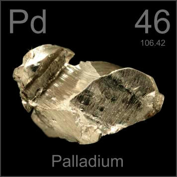
Palladium has lesser value compared to platinum and heavily relies on industrial demand behavior. For instance, palladium is expected to be a key part of the cold fusion technology that all industrialized nations are looking up to for energy solutions. Sharp investors are eager to become part of this booming technology by investing in palladium.

Related: Palladium Sputtering Target

Buying Palladium

An investor should look at reputable independent companies to buy palladium. It is available in bars and coins. For investors that want to start small, you can start with ounces or even smaller quantities.

For more information about precious metals, please visit https://www.sputtertargets.net/.

Silicon Wafer: 4 Types of Wet Cleaning Method

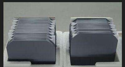
After the silicon wafer is processed by different processes such as slicing, chamfering, grinding, surface treatment, polishing, and epitaxy, the surface has been seriously stained. The purpose of cleaning the Si wafer is to remove particles, metal ions and organic substances on the surface of the silicon wafer.

Semiconductor-Silicon-Wafers

Wet cleaning uses chemical solvents with strong corrosive and oxidizing properties, such as H2SO4, H2O2, DHF, NH3•H2O, etc. The impurity particles on the surface of the silicon wafer react with the solvent to form soluble substances and gases. In order to improve the cleaning effect, it is possible to use mega-acoustic, heating, vacuum and other technical means, and finally use ultra-pure water to clean the surface of the silicon wafer to obtain a silicon wafer that meets the cleanliness requirements.

There are several methods for wet cleaning the silicon semiconductor wafer:

RCA Cleaning for Silicon Wafer

Kern et al. proposed the RCA cleaning method in 1965. According to the SPM, DHF, SC-1, and SC-2 sequences, the RCA cleaning method basically satisfies the requirements of most wafer cleanliness. Cleaning the silicon wafers by this method not only improves the cleaning efficiency, reduces the cost, saves time, obtains excellent surface cleanliness, but also improves the electrochemical performance of the Si wafer.

Ultrasonic Cleaning for Silicon Wafer

Ultrasonic cleaning is a cleaning method widely used in the semiconductor industry. The method has the advantages of good cleaning effect, simple operation, and can be removed for complicated devices and containers; but the method also has the disadvantages of high noise and easy breakage of the transducer.

This method can effectively remove organic, particulate, and metal ion impurities on the surface of the silicon wafer by utilizing the mechanical action of high-frequency sound waves, the cavitation effect of the solution, and the complexation reaction of chemical reagents. Using a similar method, BongKyun et al. used a 0.83 MHz megasonic wave to clean the silicon wafer, which is more excellent and can remove particulate impurities below 0.3 μm.

Silicon Wafer Wet Cleaning

Double Flow Spray for Silicon Wafer

The dual-flow atomizing nozzle cleans the silicon wafer by using a nozzle to scan the silicon wafer back and forth with the rotating arm, and the silicon wafer rotates clockwise. The dual-flow nozzle uses a high-pressure, high-speed jet of gas to impinge a vulgar flow of liquid, destroying the surface tension of the liquid and the van der Waals bond and hydrogen bond between the liquid molecules, causing the liquid to atomize and become nanometer-sized droplets, which are ejected at high speed through the nozzle under the action of high pressure air.

Ozone Microbubble Method for Silicon Wafer

The high activity and strong oxidizing properties of ozone can remove organic and particulate impurities on the surface of the Si wafers. Ozone is dissolved in water to form a highly reactive OH group, and the OH group chemically reacts with the organic substance to remove organic impurities on the surface of the silicon semiconductor wafer. At the same time, the surface of the silicon product is covered with an atomic-level smooth oxide film, which effectively isolates the re-adsorption of impurities.

This method has an excellent cleaning effect, basically removes organic and particulate impurities, and meets the requirements of general silicon wafer cleanliness. At the same time, ozone microbubble cleaning produces less polluting waste and high cleaning efficiency, and can be used for cleaning large-scale circuits, silicon wafers and LEDs.

For more information, please visit https://www.sputtertargets.net/.
Sputter Targets for the Chip Industry

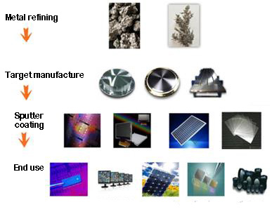
Every era has some materials to follow the mainstream trend to become the leader in the industry. Under the current situation, the development of the chip industry as a high-tech commanding point has important strategic significance, and the sputter target is a necessary raw material for the manufacture of ultra-large-scale integrated circuits. Therefore, the sputtering target material may be representative of the material emerging from this mainstream trend.

In the chip industry, which is a high-tech high point, sputter targets are essential raw materials for the manufacture of very large scale integrated circuits. Very large scale integrated circuits are those with more than 100,000 components integrated on a single chip, or more than 10,000 gates. With this technology, an electronic subsystem and even the entire electronic system can be “integrated” on one chip to complete various functions such as information collection, processing, and storage. What is repeatedly used in the manufacturing process of ultra-large-scale integrated circuits is the sputtering process belonging to physical vapor deposition (PVD) technology, which is also one of the main techniques for preparing electronic thin film materials.

The principle of the sputtering process is to utilize the ions generated by the ion source to accelerate the polymerization into a high-speed ion current in a vacuum to bombard the solid surface, and the kinetic energy exchange between the ions on the surface of the ion and the solid surface causes the atoms on the solid surface to leave the target and deposit on the substrate to form a nano/micro film.

The bombarded solid is the sputtering target, which is simply like a printing mold. The quality of the target plays a crucial role in the performance of the film, which directly determines the quality and performance of downstream semiconductor chips, flat panel displays, solar cells and other electronic devices or optical components. Therefore, the sputter target is the key raw material in the whole process.

Sputtering targets can be classified according to their chemical composition, geometry and field of application. Targets with different compositions (aluminum, copper, stainless steel, titanium, nickel targets, etc.) can be divided into different film systems (superhard, wear-resistant, anti-corrosion alloy films, etc.); if divided according to their application fields, they can be divided into It is recording medium targets, semiconductor targets, display film targets, superconducting targets, and optical targets.

The target production process includes two processes of “material purification” and “target preparation”. During the purification process, it is necessary to ensure the reduction of impurity content in the target, and the preparation process needs to ensure the surface level of the sputter coater target.

Sputtering targets for high-end applications have very high technical thresholds and are very complex to prepare. First of all, it is necessary to carry out process design according to performance requirements, and then carry out repeated plastic deformation, heat treatment, precise control of grain, crystal orientation and other indicators, and then through welding, machining, cleaning and drying, vacuum packaging and other processes.

For more information, please visit https://www.sputtertargets.net/.