Image Gallery of SAM Evaporation Materials

High purity evaporation materials play a huge role in deposition processes to ensure high quality deposited film. Stanford Advanced Materials provides various evaporation materials for both thermal and e-beam evaporation, including metal and ceramic boats, filaments, crucibles and heaters, and e-beam crucible liners.

Introduction to Two Important Vacuum Coating Methods

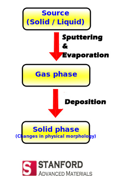
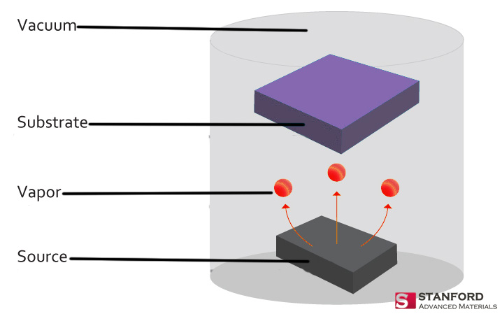
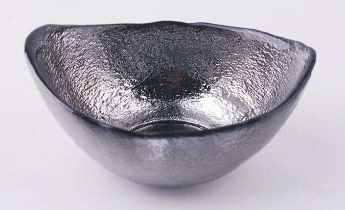
In today’s electronics industry, many electronic components are manufactured using a vacuum coating process. Vacuum coating has become an indispensable technology for the manufacture of electronic components. The current vacuum coating technology is to evaporate and sputter a metal or alloy in a vacuum to deposit it on a substrate. Vacuum evaporation and magnetron sputtering coating are two main vacuum coating technologies.

Vacuum evaporation

History

In 1857, Michael Faraday first proposed the basic principle of vacuum evaporation. Later, in the 1930s, the oil diffusion vacuum pump was put into practical use, and it was mainly used to make the lens anti-reflection film. During the Second World War, the demand for materials from other optical machines increased, and vacuum evaporation also developed rapidly.

Principle

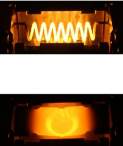
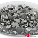
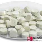
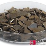
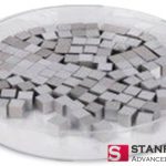
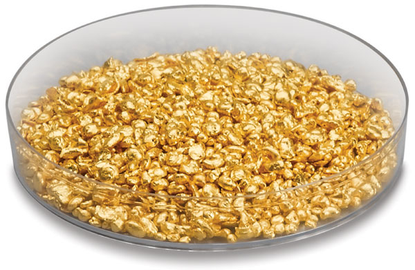
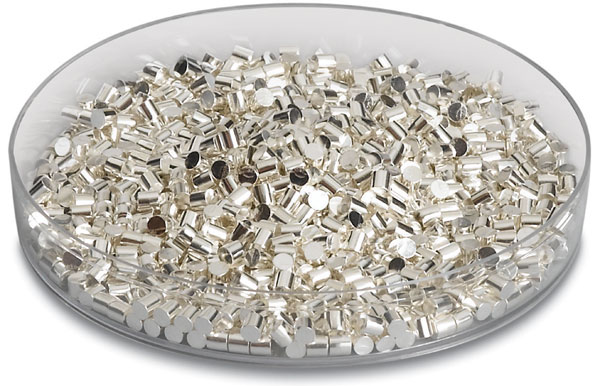
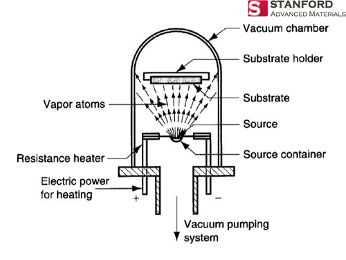
In a vacuum state, the evaporation pellets in the evaporation vessel is heated to cause atoms or molecules to escape and deposit on the surface of the evaporation material to form a solid film. Depending on the type of vapor deposition material or substrate, it can be classified into heating methods such as resistance heating, electron beam, high-cycle induction, and laser. The vapor deposition materials include metal evaporation materials such as aluminum, lead, gold, silver, platinum, and nickel, and materials capable of producing optical properties, and oxides and fluorides such as SiO2, TiO2, ZrO2, and MgF2 are mainly used. In addition to metal, vapor deposition can be used for resin and glass, and in recent years, continuous paper has also become vapor-depositable.

Advantages

The device is simple and easy to operate; the film formation rate is fast and the efficiency is high.

Disadvantages

The thickness uniformity of the film is not easy to control, the evaporation container has hidden dangers, the process repeatability is not good, and the adhesion is not high.

Magnetron sputtering coating

History

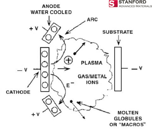
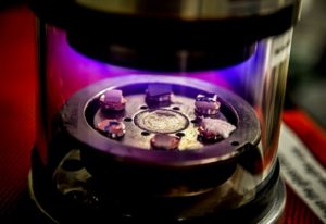
As a very effective thin film deposition method, magnetron sputtering technology has been widely and successfully applied in many fields, especially in the fields of microelectronics, optical films and material surface treatment, for thin film deposition and surface coating preparation. In 1852, Grove first described the physical phenomenon of sputtering. In the 1940s, sputtering technology began to be applied and developed as a deposition coating method. With the rapid rise of the semiconductor industry in the 1960s, this technology was widely used and widely used in the integrated circuit production process for depositing metal electrode layers of transistors in integrated circuits. The emergence and development of magnetron sputtering technology, and the use of reflective layers for CD production in the 1980s, the field of application of magnetron sputtering technology has been greatly expanded, and gradually become a common means of manufacturing many products, and in the last ten years, a series of new sputtering techniques were developed.

Principle

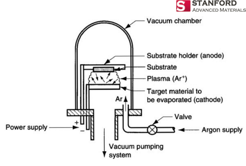
Electrons accelerate to the substrate under the action of an electric field. In this process, electrons collide with argon atoms to ionize a large amount of argon ions and electrons. Under the action of an electric field, argon ions accelerate the bombardment of the sputtering target, and sputter a large number of target atoms, and the target atoms are deposited on the surface of the substrate to form a film.

Advantages

The process repeatability is good, the film has high purity, uniform film thickness and good adhesion.

Disadvantages

The structure of the device is complicated, and once the sputtering target penetrates, the entire target is scrapped, so the utilization rate of the target is low. Using rotatory sputtering target can increase the utilization of the target.

Please visit https://www.sputtertargets.net/ for more information.

Physical Vapor Deposition: Sputter Coating & Evaporation

Physical vapor deposition processes use vacuum technology to create a sub-atmospheric pressure environment and an atomic or molecular condensable vapor source (from a solid or liquid surface) to deposit thin films and coatings. Sputtering deposition and vacuum evaporation are among the more well known.

physical vapor deposition sputtering evaporation

Sputtering deposition

The sputtering deposition is an etching process that alters the physical properties of a surface. In this process, a gas plasma discharge is set up between two electrodes: a cathode plating material (the sputter coater targets) and an anode material (the substrate). The film made by sputter coating are thin, ranging from 0.00005 – 0.01 mm. Chromium, titanium, aluminum, copper, molybdenum, tungsten, gold, and silver are typical sputter coating targets.

Sputter coated films are used routinely in decorative applications such as watchbands, eyeglasses, and jewelry. Also, the electronics industry relies on heavily sputtered coatings and films, such as thin film wiring on chips and recording heads as well as magnetic and magneto-optic recording media. Companies also use sputter deposition to produce reflective films for large pieces of architectural glass used in the automotive industry. Compared to other deposition processes, sputter deposition is relatively inexpensive.

vacuum coating

Vacuum Evaporation

The vacuum evaporation is a process of reducing the wastewater volume through a method that consists of concentrating a solution by eliminating the solvent by boiling. In this case, it is performed at a pressure lower than atmospheric pressure. Thus, the boiling temperature is much lower than that at atmospheric pressure, thereby resulting in notable energy savings. The basic components of this process consist of: evaporation pellets,  heat-exchanger, vacuum, vapor separator, and condenser.

Vacuum evaporation is used in the semiconductor, microelectronics, and optical industries and in this context is a process of depositing thin films of material onto surfaces. High-purity films can be obtained from a source evaporation material with high purity. The source of the material that is going to be vaporized onto the substrate can be a solid in any shape or form (usually pellets). The versatility of this method trumps other deposition processes. Also, when the deposition is not desired, masks are utilized to define the areas on the substrate for control purposes.

Information from Stanford Advanced Materials. Please visit https://www.sputtertargets.net/ for more information.

Evaporation Pellets for Thin Film Coating

Gold (Au) Evaporation Materials

Evaporation pellets are evaporation materials for vacuum evaporation coating.

Evaporation is a form of physical vapor deposition (PVD) where the evaporation material is heated to a high vapor pressure, often in a molten state. The vapors are then condensed on the substrate to form a thin film.

The most common heating method for vacuum evaporation is the resistance heating method. The advantages of resistance heating method include simple structure, low cost and convenient operation. The disadvantage is that it is not suitable for refractory metals and high temperature resistant dielectric materials. Electron beam heating and laser heating can overcome the shortcomings of resistance heating. Electron beam heating uses a focused electron beam to directly heat the bombarded material, and the kinetic energy of the electron beam becomes thermal energy, causing the material to evaporate. Laser heating uses a high-power laser as a heating source, but due to the high cost of high-power lasers, it can only be used in a few research laboratories. You can refer to Five evaporation sources for heating for detailed information of the heating methods. As for a thin film precious metal coating, the heating is typically accomplished via resistive heating or by E-beam (electron beam).

Evaporation pellets or slugs are manufactured with specific form factors intended to vaporize at known rates. Often during evaporation processes, “spitting” results in liquid droplet material splattering on to the substrate. Engineered pellets are made with specified metal purities and processes intended to minimize incorporated gases and impurities to mitigate “spitting” in process.

Silver (Ag) Evaporation Materials

Optimal evaporative performance for thin film deposition is highly dependent on the use of high purity materials specifically customized for PVD processes. It requires evaporation materials that feature low organic and inorganic impurities, as well as minimal surface contamination. This level of purity results in highly reproducible performance with low spit rates and defects. SAM offers high-quality evaporation materials in precious metals for your PVD coating.

The following chart shows some common thin film deposition of precious metals. SAM can customize any precious metal alloy you need that is not listed.

 Gold Copper Gold Nickel Gold Nickel Indium
Gold Palladium Gold Gold Silicon
Gold Silver Platinum Gold Tin Gold Zinc
Palladium Rhenium Palladium Lithium Palladium Manganese
Palladium Nickel Platinum Palladium Platinum Iridium
Platinum rhodium Silver Gold Silver Titanium

Please visit https://www.sputtertargets.net/evaporation-materials.html for more information.

Introduction to Physical Vapor Deposition Technologies

Thin Film Deposition

Thin film deposition technology refers to the preparation of thin films on the surface of materials used in the fields of machinery, electronics, semiconductors, optics, aviation, transportation and etc., in order to impart certain properties (such as heat resistance, wear resistance, corrosion resistance, decoration, etc.) to these materials.

The two most common forms of thin film deposition techniques are physical vapor deposition (PVD) and chemical vapor deposition (PVD).

Physical Vapor Deposition —PVD

PVD is a process that achieves the transformation of the atoms from the source materials to the substrate to deposit a film by physical mechanisms such as thermal evaporation or sputtering.

PVD includes evaporation, sputtering and ion plating.

Evaporation

Evaporation is a common method of thin-film deposition. It is also called vacuum evaporation because the source material is evaporated in a vacuum. The vacuum allows the vapored particles to travel directly to the substrate, where they condense and deposit to form a thin film.

Evaporation (PVD)
Evaporation (PVD)

Sputtering

Sputtering is a physical vapor deposition (PVD) method of thin film deposition. It is a process whereby particles are ejected from a solid target material (sputtering target) due to the bombardment of the target by energetic particles.

Sputtering (PVD)
Sputtering (PVD)

Ion Plating

Ion plating is a physical vapor deposition (PVD) process which uses a concurrent or periodic bombardment of the substrate, and deposits film by atomic-sized energetic particles.

Ion Plating (PVD)
Ion Plating (PVD)

Characteristics of the main physical vapor deposition method

Among the above three methods, although Ion plating’s film adhesion and density are better, due to technical limitations, the other two methods (evaporation and sputtering) are currently more widely used. In general, sputtering is the best PVD technology.

Stanford Advanced Materials (SAM) is one of the most specialized sputtering targets manufacturers, please visit https://www.sputtertargets.net/ for more information.

Deposition of silver on glass by e-beam evaporation

The case

I am attempting to use silver evaporation pellets to deposit one-micrometer thick silver layer on the glass substrate. I found that only electron beam evaporation is accessible within the facility. I tried Ag/Ti/glass but silver peels off the Titanium layer. Up to now, only Ag/Au/Ti/glass can partially work, and only 1/2 of my samples were fully coated with silver; the other half turned into blackish-rainbow color. I wonder what is wrong in the process? Should I should some intermediate layers?

Possible Cause and Solution

The thickness of the Titanium (Ti) layer may be too large. Generally speaking, 5 to 10 nm is enough in this case.

The process is not operated in a good vacuum condition, thus the titanium layer is oxidized. In electron beam evaporation, as well as other vacuum evaporation, the vacuum degree of the evaporator is extremely important, which will greatly influence the quality of the film obtained. Thus, please make sure the vacuum chamber is well sealed before evaporating.

It is hard to avoid that the evaporated silver (as well as gold) only loosely connected to the glass substrate. Cleaning the glass with acetone and then methanol could help. Or you can just replace the glass substrate by using another transparent substrate, such as Al2O3, SiO2, AlN and Diamond. The silver layer can better deposit on those substrates mentioned above.

Other Suggestions

Titanium is an excellent adhesion layer, but it is also true that it may lose some of its adhesiveness if the vacuum is not good enough. As for its alternatives, Chromium (Cr) and Aluminum (Al) are recommended to act as the adhesion promoter.

Rising the temperature up to 100℃ in the vacuum for a few minutes may also improve the adhesion of metals.

Silver (Ag) Evaporation Materials

For the explanation of the terminologies of vacuum coating mentioned in this passage, please refer to Terminologies of Vacuum Evaporation.

For high purity silver evaporation materials, please visit Stanford Advanced Materials.

For more news and knowledge about vacuum coating, please see SAM News.

PVD vs. CVD: What’s the difference?

PVD vs. CVD: What’s the difference?

In recent years, physical vapor deposition (PVD) and chemical vapor deposition (PVD) have wide applications in various industries to increase the hardness of tools and molds or apply beautiful colors to the products. Thus these two methods are considered as the most attractive surface coating technologies. Then, using the example of cutting tools, let’s make a detailed comparison between these two methods.

Definition

Physical vapor deposition (PVD) uses low-voltage, high-current arc discharge technology under vacuum conditions to evaporate the target and ionize the vaporized material and the gas, and finally make the evaporated material and its reaction deposited on the workpiece.

Continue reading “PVD vs. CVD: What’s the difference?”

Differences between vacuum evaporation and sputter coating

It is well known that vacuum coating has two common methods: vacuum evaporation and sputter coating. However, many people have doubts about the difference between evaporation and sputter coating. Let SAM Sputter Targets answer it for you.

sputter coating3First, let’s take a look at the definition of these two words. The vacuum evaporation is carried out by means of resistance heating, electron beam or laser bombardment in an environment with a vacuum of not less than 10-2 Pa, and the evaporation material is heated to a certain temperature to evaporate or sublimate a large number of molecules or atoms, and then directly deposited on a substrate to form a film. Continue reading “Differences between vacuum evaporation and sputter coating”

Five evaporation sources for heating

The evaporation source is a heating element used to vaporize  the molding material. The evaporation sources currently used mainly include the following types:

Resistance evaporation heating source

The resistance heating method is simple and easy to operate, and is a common application method: a filament-like or sheet-like high melting point metal (such as Tungsten, Molybdenum, Titanium, etc.) is made into an evaporation source of a suitable shape. It is equipped with an evaporation material to turn on the power supply, and the evaporation material is directly heated and evaporated. The resistance heating method should mainly consider two problems, the melting point and vapor pressure of the evaporation material; the reaction of the evaporation material with the coating material and the wettability caused by the coating material.

Electron beam evaporation source

The evaporation material is placed in a water-cooled copper dry pot and directly heated by an electron beam, which is called electron beam heating. It can vaporize the evaporation material and form a film on the surface of the substrate. It is an important heating method and development direction in the vacuum evaporation coating technology. In the resistance heating method, the coating material and the evaporation material are in direct contact, and the temperature of the evaporation material is higher than that of the coating material, and is easily mixed into the coating material, especially in the semiconductor device coating. Electron beam evaporation can overcome many shortcomings of general resistance heating evaporation, and is particularly suitable for preparing high melting point film materials and high purity film materials.

High frequency induction heating evaporation source

The high-frequency induction heating evaporation source places the graphite or quartz crucible containing the evaporation material in the center of the water-cooled high-frequency spiral coil, so that the evaporation material generates strong eddy current loss and hysteresis loss under the induction of the magnetic field in the high frequency band (to Ferromagnetic), causing the evaporating material to heat up until evaporation. The smaller the volume of the evaporated material is, the higher the frequency of induction is. In the large-scale vacuum aluminum plating equipment on the steel strip, the high-frequency induction heating evaporation process has achieved great success.

Radiant heating evaporation source

For materials with high absorption of infrared radiation, it can be evaporated by radiant heating, and many substances are evaporated by this method. In addition, the reflectivity of the metal for infrared radiation is high, and the absorption rate of quartz for infrared radiation is low, so they are difficult to be evaporated by radiation heating. The main advantage of the radiant heating method is that the evaporation is only heated on the surface, and the adsorbed gas is released on the surface without splashing the material.

Laser beam evaporation source

The evaporation technique using a laser beam evaporation source is an ideal film preparation method because the laser can be installed outside the vacuum chamber. This not only simplifies the space arrangement inside the vacuum chamber and reduces the abandonment of the heating source, but also completely avoids the contamination of the evaporation material by the evaporator, thus it is advantageous for obtaining a high-purity film.


Stanford Advanced Materials (SAM) Corporation is a global supplier of various sputtering targets such as metals, alloys, oxides, ceramic materials. If you are interested, please visit our website https://www.sputtertargets.net/ for more information.