Platinum and palladium are in the class of precious metals just like gold and silver in spite of little information concerning their investments. The difference is that they are not in form of currency because they are in form of industrial metal, and belong to a group called platinum metals group.
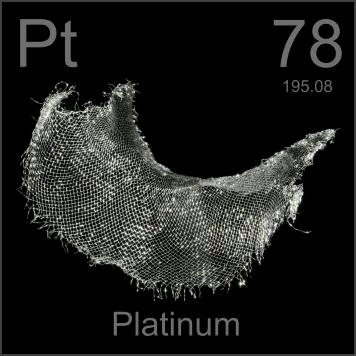
Platinum
The fact that platinum is not a monetary metal confers advantages and disadvantages alike. First, it can be affected by demand issues due to its industrial nature and hence suffer massive price fluctuations sue to speculation. Secondly, it does not have the global attraction that gold and silver have as monetary metals. However, the fact that it non-monetary ensures that it is not targeted for confiscation as is the case with silver and gold. Second, the historic hart of the metal has shown that its price goes hand in hand with gold value over time even though it is more of an industrial metal. This tells you that it is a worth investment.
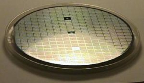
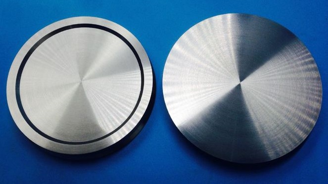
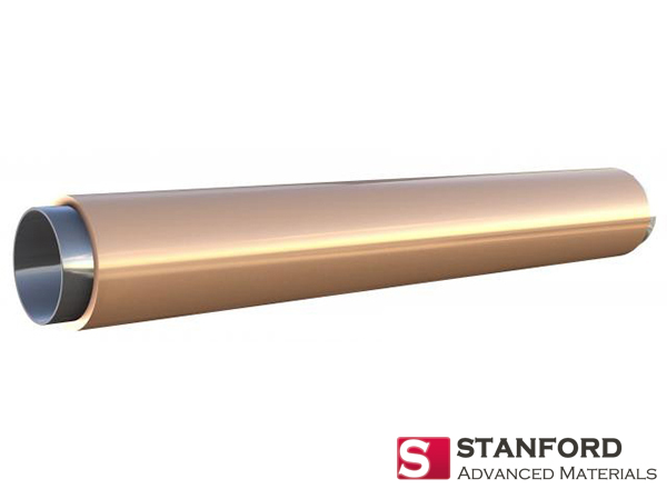
Related: Platinum Sputtering Target
Ways to Buy Platinum
There are a number of reputable dealers that can be contacted online. These dealers have established stores in Hong Kong, Switzerland or London. You can buy in small quantities from independent but reputable companies. For bulk buying, ensure that there is an arrangement for adequate storage because safety is of great importance. Second, you can explore mints that can produce bullion coins in the U.S, Canada, Australia, and China. The coins are available in the denominations between a tenth of an ounce and one troy ounce. Collectors tend to be more expensive than mints since most coins are regarded as collector’s items. Finally, you can consider collecting old or scrap platinum jewelry from second hand or coin shops. Another advantage of buying platinum jewelry is the authenticity and purity that comes with them.
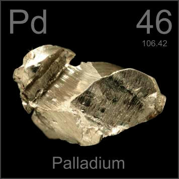
Palladium
Palladium has lesser value compared to platinum and heavily relies on industrial demand behavior. For instance, palladium is expected to be a key part of the cold fusion technology that all industrialized nations are looking up to for energy solutions. Sharp investors are eager to become part of this booming technology by investing in palladium.
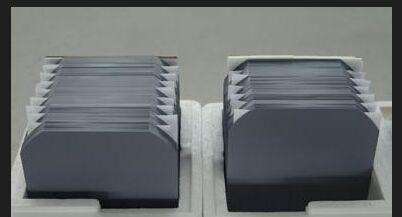
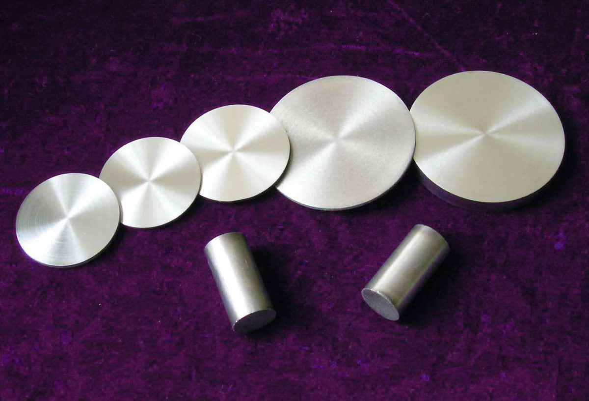
Related: Palladium Sputtering Target
Buying Palladium
An investor should look at reputable independent companies to buy palladium. It is available in bars and coins. For investors that want to start small, you can start with ounces or even smaller quantities.
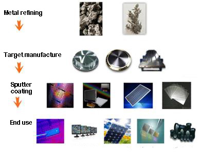
For more information about precious metals, please visit https://www.sputtertargets.net/.