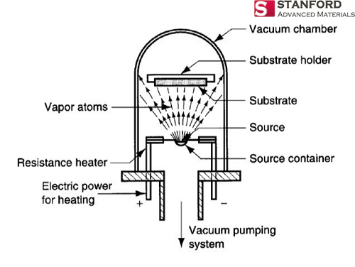
Thermal evaporation, or vacuum evaporation, refers to the vaporization of evaporation materials. By heating evaporation materials to a certain temperature, the vapor pressure becomes appreciable, and the surface or molecules are lost from the surface in the vacuum. Vaporization can come from the surface of a liquid or from the surface of a solid. The equilibrium vapor pressure (EVP) is 10-2 Torr. Some evaporation materials have a vapor pressure so that they can sublime or evaporate (e.g., titanium) at temperatures near their melting points. Some composites sublime and some evaporate.

From late 1800s to early 1900s
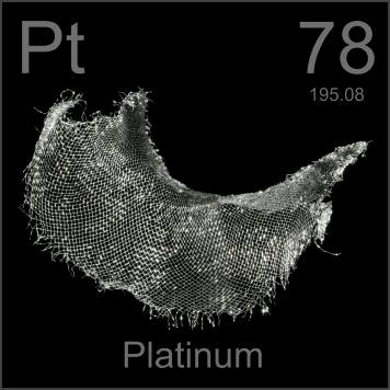
In 1887, Nahrwold reported the formation of platinum thin films by subliming platinum evaporation materials in a vacuum. Therefore, some believe that he was the first to use thermal evaporation to form thin films in a vacuum.
In 1907, Soddy proposed that it would be possible to evaporate solid calcium onto the surface to reduce the residual pressure in the sealed tube. This is believed to be the first “reactive deposition” process in history.
In 1909, Knudsen proposed the “Knudsen Cosine Distribution Law” for vapor from a point source. After 6 years, he refined the free surface evaporation rate as a function of equilibrium vapor pressure and ambient pressure. The resulting equation is called the Hertz-Knudsen surface equation for free-surface vaporization. Honig summarized the equilibrium vapor pressure data for 1957.
From the early 1900s to the mid-1900s
In 1912, von Pohl and Pringsheim reported the formation of thin films by evaporating solid materials in a vacuum using a magnesia crucible as a container. Their experiments are sometimes considered the first thin-film deposition by thermal evaporation in a vacuum.
In 1931, Ritschl reported thermal evaporation of silver from a tungsten wire basket to form half-silvered mirrors. And he is often credited with being the first to use evaporation from a filament to form a film in a vacuum.
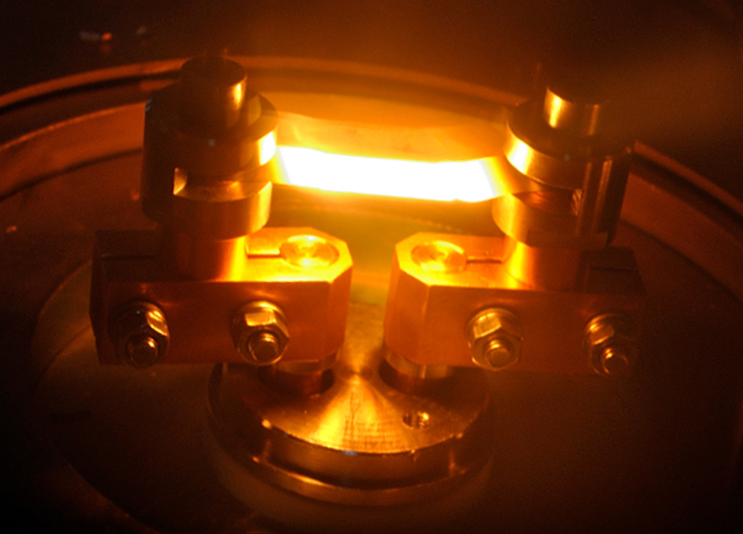
Evaporating Aluminum Thin-Film
Cartwright and Strong reported on the evaporation of metals from tungsten wire baskets in the same year. However, their attempts to vaporize aluminum failed, because molten aluminum would wet with the tungsten filament to form an alloy, which causes it to “burn out” when there is a relatively large volume of molten aluminum.
Aluminum thin films were not successfully produced by vacuum evaporation until 1933, when John Strong used large gauge tungsten filaments wetted by molten aluminum. John has done extensive development work for astronomical mirror coatings using the aluminothermic evaporation of multiple tungsten wires. Strong, with the help of designer Bruce Rule, used multiple filaments and a 19-foot diameter vacuum chamber to aluminize the 200-inch Palomar telescope mirror in 1947.
AR Coating
In 1933 A.H. Pfund vacuum-deposited the first single-layer (AR) coating (ZnS) while reporting on making beamsplitters and Bauer mentioned AR coatings in his work on the properties of alkali halides.
The Germans deposited CaF2 a nd MgF2 AR coatings during WWII. Plasma cleaning of glass surfaces is reported to have been used by Bauer at the Zeiss Company in 1934. The Schott Company (Germany) was also reported to have deposited three-layer AR coatings by flame-pyrolysis CVD during WWII.
In 1935, based on Bauer’s observation, A. Smakula of the Zeiss Company developed and patented AR coatings on camera lenses. The patent was immediately classified as a military secret and was not revealed until 1940.
In1936, Strong reported depositing AR coatings on glass.
In 1939, Cartwright and Turner deposited the first two-layer AR coatings.
One of the first major uses of coated lenses was on the projection lenses for the movie Gone With the Wind, which opened in December 1939. The AR-coated lenses gained importance in WWII for their light-gathering ability in such instruments as rangefinders and the Norden Bombsight.
The AR coated lenses gained importance in WWII for their light-gathering ability in such instruments as rangefinders and the Norden Bombsight. During WWII, baking of MgF2 films to increase their durability was developed by D.A. Lyon of the U.S. Naval Gun Factory. The baking step required that the lens makers coat the lens elements prior to assembly into compound lenses.
In 1943, the U.S. Army sponsored a conference on “Application of Metallic Fluoride Reflection Reducing Films to Optical Elements.” The proceedings of this conference are probably the first extensive publication on coating optical elements.
In 1958, the U.S. military formally approved the use of “vacuum cadmium plating” (VacCad) for application as corrosion protecmium. In recent years Physical Vapor Deposition (PVD) methods have been used to replace electroplating in a number of applications to avoid the water pollution associated with electroplating.
From the mid-1900s to the late 1900s
E-beam Evaporation Development
In 1949, Pierce described the “long-focus” electron beam gun for melting and evaporation in a vacuum. The long focus gun suffers from shorting due to the deposition of evaporated material on the filament insulators that are in the line of sight of the evaporating material. Deposition rates as high as 50 µm/s have been reported using e-beam evaporation. To avoid exposure of the filament to the vapor flux, bent-beam electron evaporators were developed.
In 1951, L. Holland patented the use of accelerated electrons to melt and evaporate the tip of a wire (“pendant drop”), which involved no filament or crucible.
In 1968, Hanks filed a patent on a 270° bent beam electron beam evaporation source that has become the most widely used design. Mastering the electron beam allows the energy of the electron beam to be distributed over the surface.
In 1970, Kurz was using an electron-beam system to evaporate gold for web coating. In electron beam evaporation a high negative “self-bias” can be generated on the surface of an insulating material or on an electrically isolated fixture. This bias can result in high-energy ion bombardment of the self-biased surface.
In 1971, Chambers and Carmichael avoided that problem by having the beam pass through a small hole in a thin sheet in a section of a plate that separated the deposition chamber from the chamber where the filament was located. This allowed a plasma to be formed in the deposition chamber while the filament chamber was kept under a good vacuum. The plasma in the deposition chamber allowed ion bombardment of the depositing film material as well as “activation” of reactive gas.
In 1972, the use of a hollow cathode electron emitter for e-beam evaporation was reported by J.R. Morley and H. Smith.
In 1978 H.R. Smith described a unique horizontally emitting electron beam (EB) vapor source. The source used a rotating crucible to retain the molten material, and its function was to coat large vertical glass plates. A number of thermoelectron-emitter e-beam source designs followed, including rod-fed sources and “multi-pocket” sources. The high voltage on the filament prevented the source from being used in a plasma where ions accelerated to the cathodic filament; this caused rapid sputter-erosion of the filament.
Crucible material Development
In 1951 Picard and Joy described the use of evaporation of materials from an RF-heated crucible. In 1966 Ames, Kaplan, and Roland reported the development of an electrically conductive TiB/BN composite ceramic (Union Carbide Co., UCAR™) crucible material that was compatible with molten aluminum.
Directed Deposition Development
The directed deposition is confining the vapor flux to one axis by eliminating off-axis components of the flux. Directed deposition can be attained by the collimation of the vaporized material. This was done in evaporation by Hibi (1952), who positioned a tube between the source and the substrate. Collimation was also attained by H. Fuchs and H. Gleiter in their studies of the effects of atom velocity on film formation using a rotating, spiral-groove, velocity selector.
In 1983, Ney described a source that emitted a gold atom beam with a 2° divergence. Recently, “directed deposition” has been obtained using a flux of thermal evaporated material projected into a directed gas flow.
Thermally Evaporating Development
When thermally evaporating alloys, the material is vaporized with a composition in accordance with Raoult’s Law (1887). This means that the deposited film will have a continuously varying composition unless very strict conditions are met as to the volume of the molten pool using a replenishing source. One way of avoiding the problem is by “flash evaporation” of small volumes of material.
In 1948, L. Harris and B.M. Siegel reported flash evaporation by dropping small amounts of material on a very hot surface so that all of the material was vaporized before the next material arrived on the hot surface.
In 1964, Smith and Hunt described a method for depositing continuous strips of alloy foils by evaporation. Other free-standing thin-film structures are also deposited, such as beryllium Xray windows and nuclear targets.
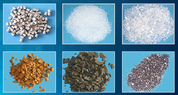
To learn more about the history of thermal evaporation, please follow our website. We will update articles about evaporation pellets every week, so stay tuned. If you want to buy high-quality evaporating pellets, please visit our official website for coating materials at https://www.sputtertargets.net/.