How was Silicon discovered? | History of Silicon

Silicon

Discovery of Silicon

In 1787, the French chemist Antoine-Laurent de Lavoisier first discovered the silicon present in rocks. In 1800, silicon was mistaken by Sir Humphry Davy as a compound. In 1811, French chemists Joseph Louis Gay-Lussac and Louis Jacques Thénard probably prepared impure amorphous Silicon by heating potassium with silicon tetrafluoride. They later named it silicon according to the Latin silex (meteorite).

Until 1823, silicon was first discovered in the form of a metal element by the Swedish chemist Jöns Jacob Berzelius. One year later, he extracted amorphous silicon in much the same way as Gay-Lussac, and then purified the elemental silicon by repeated cleaning; in the same year, he heated the silicon oxide powder and the mixture of iron and carbon at a high temperature and obtain the iron silicide.

In order to extract pure silicon, Berzelius dry-fired the silicon-fluorine-calcium compound, hydrolyzed the obtained solid, and manage to obtain the pure silicon. In 1824, in Stockholm, Berzelius obtained relatively pure silicon powder by heating potassium fluorosilicate and potassium. Therefore, it is agreed that the honor of discovering silicon belongs to Berzelius.

Properties of Silicon

Symbol: Si
Atomic Number: 14
Atomic Weight: 28.09
Element Category: metalloid
Color: dark gray with a bluish tinge
Density: 2328.3 kg/m³
Hardness: 6.5
Proportion in Earth’s Crust: 25.7%
Other Names: Silicium, Silicio

Application of Silicon

High-purity monocrystalline silicon is an important semiconductor material that can be used as a solar cell to convert radiant energy into electrical energy, which is a promising material in the development of energy.

Silicon can also be made into cermet composites, which are resistant to high temperatures, toughness, and can be cut. They not only inherit the respective advantages of metals and ceramics, but also make up for the inherent defects of both, and can be applied to weapons manufacturing and aerospace.

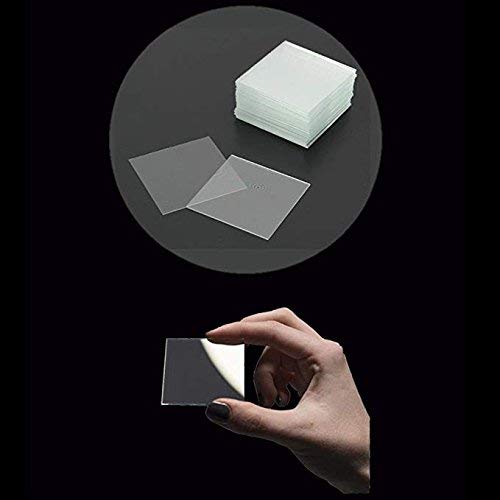
Pure silica can be used to draw high transparency glass fiber for optical fiber communication, which is the latest modern communication means.

Please visit https://www.sputtertargets.net/ for more information.

Introduction to Physical Vapor Deposition Technologies

Thin Film Deposition

Thin film deposition technology refers to the preparation of thin films on the surface of materials used in the fields of machinery, electronics, semiconductors, optics, aviation, transportation and etc., in order to impart certain properties (such as heat resistance, wear resistance, corrosion resistance, decoration, etc.) to these materials.

The two most common forms of thin film deposition techniques are physical vapor deposition (PVD) and chemical vapor deposition (PVD).

Physical Vapor Deposition —PVD

PVD is a process that achieves the transformation of the atoms from the source materials to the substrate to deposit a film by physical mechanisms such as thermal evaporation or sputtering.

PVD includes evaporation, sputtering and ion plating.

Evaporation

Evaporation is a common method of thin-film deposition. It is also called vacuum evaporation because the source material is evaporated in a vacuum. The vacuum allows the vapored particles to travel directly to the substrate, where they condense and deposit to form a thin film.

Evaporation (PVD)
Evaporation (PVD)

Sputtering

Sputtering is a physical vapor deposition (PVD) method of thin film deposition. It is a process whereby particles are ejected from a solid target material (sputtering target) due to the bombardment of the target by energetic particles.

Sputtering (PVD)
Sputtering (PVD)

Ion Plating

Ion plating is a physical vapor deposition (PVD) process which uses a concurrent or periodic bombardment of the substrate, and deposits film by atomic-sized energetic particles.

Ion Plating (PVD)
Ion Plating (PVD)

Characteristics of the main physical vapor deposition method

Among the above three methods, although Ion plating’s film adhesion and density are better, due to technical limitations, the other two methods (evaporation and sputtering) are currently more widely used. In general, sputtering is the best PVD technology.

Stanford Advanced Materials (SAM) is one of the most specialized sputtering targets manufacturers, please visit https://www.sputtertargets.net/ for more information.

A Summary of the Titanium Alloy Properties

SAM®Titanium is a new type of metal. Its properties are related to the content of other impurities, such as carbon, nitrogen, hydrogen and oxygen. The purest titanium iodide has an impurity content of less than 0.1%, but it has low strength and high plasticity.

The general properties of 99.5% industrial pure titanium are as follow:

Stanford Advanced Materials
density ρ 4.5g/cm3
melting point 1725°C
thermal conductivity λ 15.24W/(mK)
tensile strength σb 539MPa
elongation δ 25%
section shrinkage ratio ψ 25%
elastic modulus E 1.078×10⁵ MPa
hardness HB 195

(1) High specific strength

The density of titanium alloy is generally about 4.5g/cm3 (only 60% of steel), but the strength of pure titanium is close to that of normal steel. And some high-strength titanium alloys have higher strength than many alloy structural steels. Therefore, the specific strength (strength/density) of titanium alloy is much larger than that of other metal structural materials. It can be used to produce parts and components with high unit strength, good rigidity and lightweight. At present, titanium alloys are used for aircraft engine components, skeletons, skins, fasteners and landing gear.

Titanium Aeroplane Engine

(2) High-temperature strength

Titanium alloys can be used in higher temperature environments than aluminum alloys. Titanium alloys can retain the required strength and maintain long-term operation at the temperatures between 450 and 500 °C. While the specific strength of the aluminum alloy is significantly reduced when the temperature reaches 150 ° C.

(3) Good corrosion resistance

Titanium alloy can work in the moist atmosphere and seawater medium with good corrosion resistance, which is much better than stainless steel. It is especially resistant to pitting, acid etching and stress corrosion. In addition, titanium also has excellent corrosion resistance to alkali, chloride, chlorine organic substances, nitric acid, sulfuric acid, and the like. The fly in the ointment is that titanium has poor corrosion resistance to reducing oxygen and chromium salt media. For more information about the corrosion resistance of titanium, please read this passage Does titanium never corrode?

Titanium Ship
Titanium Ship

(4) Good low-temperature performance

Titanium alloys retain their mechanical properties at low and ultra-low temperatures. Titanium alloys with good low-temperature properties and extremely low interstitial elements. For instance, TA7 can retain a certain degree of plasticity at -253 °C. Therefore, the titanium alloy is also an important low-temperature structural material.

Please visit https://www.sputtertargets.net/ for more information.

Copper Sulfide Sputtering Targets Are The Best Sputtering Materials

Sputtering is a thin film deposition process in the modern technology world of CDs, semiconductors, disk drives and optical devices industries. Sputtering is the process at an atomic level, where the atoms are automatically sputtered out from the sputtering materials and then be deposited on another substrate, such as a solar panel, semiconductor wafer or optical device. It is an effect of the severe bombard of the high energy particles on the target.

In general, sputtering occurs only when kinetic energy is said to be bombarding particles at very high speeds, which is much higher than a normal thermal energy. At the atomic level, this makes thin film deposition more precise and accurate than that by melting the source material using conventional thermal energy.

Copper Sulfide is the best material for Sputtering Targets. It can be molded into the shape of Plates, Discs, Step Targets, Column Targets and Custom-made. Copper Sulfide is a combination of two materials—Copper and Sulphur. The chemical name of the product is CuS, which offers you the Copper Sulfide product with more than 99 percent purity.


CopperCyprus is the original source material for the chemical element Copper. The people of Middle East initially discovered it in 9000 BC. “Cu” is the canonical chemical symbol of copper.


SulfurWhereas Sulfur, otherwise known as sulphur, is first introduced in 2000 BC and discovered by Chinese and Indians. It is a chemical name originated from the Sanskrit word ‘sulvere’, and the Latin ‘sulfurium’. Both names are for sulfur.


Copper Sulfide metal discs and plates are highly adhesive and resistant against oxidation and corrosion. Using Copper Sulfide sputtering targets to deposit thin films will not produce highly reflective and extremely conductive films, but can also extensively increase the efficiency of the source energy.

So to achieve the desired noticeable result in a sputtering deposition, the built-up process used to fabricate the Sputtering Targets should be critical. A Copper Sulfide targeted material will give the best result. However, material like only an element, alloys, mixture of elements, or perhaps a compound can be used for the purposes.

For more information about sputtering targets, please visit http://www.sputtertargets.net/.

How to Prevent the Damage of ITO Exposure?

What is indium tin oxide

Indium Tin Oxide, or ITO, is a composition of indium, tin, and oxygen with different proportions. ITO is mainly used in the production of liquid crystal displays (LEDs), flat panel displays, plasma displays, touch displays, electronic paper applications, organic light-emitting diodes, and solar cells, and antistatic coatings as well as EMI shielding transparent conductive coating. The indium tin oxide film is typically deposited onto the surface physical vapor deposition, such as vacuum sputtering, or electron beam evaporation. Other uses for indium include: indium bonding, vehicle and aircraft bearings, cryogenic alloys and solders, and nuclear reactor control rods.

indium tin oxide film-12

ITO dust hazard

In the ITO sputtering target manufacturing factory, although the surface grinding and cutting operations are carried out in a closed wet system, droplets and waste water containing indium tin oxide sprayed around the machine are evaporated to dryness, causing the indium tin oxide dust to be suspended in the air. And the inhalation of ITO dust by the human body can cause lung disease.

Protection and precautions

  • Smash, grind, cut and sputter targets and backplate bonding areas shall have adequate and appropriate exhaust equipment.
  • During work, workers are advised to wear appropriate dust masks to avoid inhalation of indium, indium tin oxide and indium compound particles and fumes.

mask should be used in the area

  • Use appropriate eye and hand protection to prevent dust particles from splashing or touching.
  • Work clothes or dust-proof clothes should be used during work. Before going home, you should change clothes to avoid taking dust home, work clothes or dust-proof clothes in the factory.
  • Do not place drinking water and food at the work site to avoid contamination and avoid eating, and avoid eating or resting in the workplace.

The above points are strictly enforced at SAM’s factories, and we have never reported incidents of cancer caused by inhalation of harmful dust.

SAM is the world’s leading sputtering target manufacturer and we provide high-quality products and satisfying service. Please visit https://www.sputtertargets.net/ for more information.

The Self-Healing Ability of Cerium Coating (Chromium Substitute)

In recent years, several research efforts have targeted the utilization of rare earth elements, especially on cerium thin-film coatings. Cerium is a soft, ductile, and silvery-white metal that tarnishes when exposed to air, and it is so soft that can be cut with a knife. Cerium has no biological role and is not very toxic. Many surface treatments, like sol-gel, chemical vapor deposition (CVD) and physical vapor deposition (PVD) techniques, based on the use of cerium and cerium compounds have been investigated because of their low toxicity. In other words, consumption or inhalation of those compounds is not considered harmful to health.

Cerium compound physical vapor deposition permits improving corrosion protection performance of the surface on it is deposited on. The composition of the films has an impact on the corrosion properties of the cerium-based layer. In general, the coatings obtained by PVD are composed of Ce compounds in trivalent or tetravalent states. The ratio between these 2 oxidization states is strongly dependent on the oxidizing ability of the medium. However, no clear correlation between the Ce oxidation state and corrosion properties was found nowadays.

cerium film
cerium film

What’s more, these cerium coatings have an active mechanism similar to that observed for chromate coatings in that they both have the amazing self-healing ability when damage occurs. Chromate coatings have self-healing properties because of the presence of unreacted Cr6+ ions that are able to migrate to the exposed metal (for example a scratch) and can be further reduced to create a Cr3+ based compound that seals the scratch or the defect. However, the chromate compounds are extremely toxic and carcinogenic. Since cerium is not toxic, it is a perfect substitute for chromate. When it comes to cerium, the contact between a CeO2 film and solution induces the formation of Ce(OH)22+ ions. The existence of oxidizable metal would reduce these ions into Ce3+. Then the precipitation of trivalent cerium oxide occurs; it can be enhanced by the local increase of alkalinity. Therefore, this precipitated oxide seals the film and decreases the corrosion rate of the metal. Since cerium is not toxic, it is a perfect substitute for chromate.

In conclusion, cerium is good, but some people would concern about its price. Is rare earth element—Cerium—very expensive? The answer is not, actually Cerium is one of the least expensive rare earth and is the major component of “mischmetal”. So don’t care too much about the price.

For high purity sputtering targets & evaporation materials inquiries, please visit SAM Sputter Target.

For more news and knowledge about sputtering targets, please see SAM Target News.

Related Blog: How was cerium discovered? | History of Cerium

What is the Indium Bonding for Sputtering Target?

Read more: What Is Indium Bonding for Sputtering Target?

The term “indium bonding” in the thin film coating industry, simply speaking, refers to bonding two (or more) sputtering targets with indium (In), or one (or more) indium plates together.

Indium

Indium can be uniquely used in lower temperature solders, is one of the softest materials. Indium is preferred for target bonding because of its excellent thermal conductivity of all available bonds. In addition, indium is the most efficient material at drawing heat away from the sputtering target. Most materials can be indium bonded and there are just a few exceptions.

Apart from indium bonding, indium is also popular for a variety of uses and purposes, such as creating alloys, photoconductors, and thermistors.

Indium bond

Sputtering targets can be cracked, warped, or damaged due to inadequate cooling, low hardness, or other reasons. From this point of view, although target bonding does generate a fee, it can well protect your target from damage. It is especially true for those less-strong target materials and precious metal materials.

Elastomer is an alternative bonding method that touts a higher temperature capability over the indium bond. Elastomer bonds are recommended when you are consistently melting indium bonds. We also recommend elastomer bonding for low melting point target materials, as well as, temperature-sensitive compounds and targets that have either low density or are especially fragile.

indium target bonding

Indium bonding is preferred in applications where:

Cryogenic stability is needed

Sealing requires high levels of hermeticity

Maximum thermal transfer is required

Bonding to not-metallic surfaces

Flux cannot be used

Backing plates

OFHC Copper Backing Plate is another well-known backing plate. It is frequently used to bond ceramic targets because of its non-magnetism and low coefficient of thermal expansion. This metal has good electrical and thermal characteristics while also being easy to machine, easy to soften, and readily available at a low cost. Copper backing plates can be re-used, with care, 20 or more times.

A molybdenum plate is usually used to substitute copper plate if copper is not appropriate for the application. For instance, the coefficient of expansion for copper is mismatched with some ceramics. And for high-temperature bonding, copper may also oxidize badly or warp. In these conditions, molybdenum is a more suitable material.

SAM Sputter Target

If you are looking for an indium bonding manufacturer, SAM is undoubtedly your best choice. Stanford Advanced Materials is devoted to machining standard backing plates and working together with the Taiwan Bonding Company for providing bonding services. For questions about target bonding materials, methods, and services, please see our listing of frequently asked questions (FAQs).

Related blog: When do you need target bonding?

Deposition of silver on glass by e-beam evaporation

The case

I am attempting to use silver evaporation pellets to deposit one-micrometer thick silver layer on the glass substrate. I found that only electron beam evaporation is accessible within the facility. I tried Ag/Ti/glass but silver peels off the Titanium layer. Up to now, only Ag/Au/Ti/glass can partially work, and only 1/2 of my samples were fully coated with silver; the other half turned into blackish-rainbow color. I wonder what is wrong in the process? Should I should some intermediate layers?

Possible Cause and Solution

The thickness of the Titanium (Ti) layer may be too large. Generally speaking, 5 to 10 nm is enough in this case.

The process is not operated in a good vacuum condition, thus the titanium layer is oxidized. In electron beam evaporation, as well as other vacuum evaporation, the vacuum degree of the evaporator is extremely important, which will greatly influence the quality of the film obtained. Thus, please make sure the vacuum chamber is well sealed before evaporating.

It is hard to avoid that the evaporated silver (as well as gold) only loosely connected to the glass substrate. Cleaning the glass with acetone and then methanol could help. Or you can just replace the glass substrate by using another transparent substrate, such as Al2O3, SiO2, AlN and Diamond. The silver layer can better deposit on those substrates mentioned above.

Other Suggestions

Titanium is an excellent adhesion layer, but it is also true that it may lose some of its adhesiveness if the vacuum is not good enough. As for its alternatives, Chromium (Cr) and Aluminum (Al) are recommended to act as the adhesion promoter.

Rising the temperature up to 100℃ in the vacuum for a few minutes may also improve the adhesion of metals.

Silver (Ag) Evaporation Materials

For the explanation of the terminologies of vacuum coating mentioned in this passage, please refer to Terminologies of Vacuum Evaporation.

For high purity silver evaporation materials, please visit Stanford Advanced Materials.

For more news and knowledge about vacuum coating, please see SAM News.